RADIATION-HARD HIGH VOLTAGE CMOS MONOLITHIC SENSORS
Since 2013 we are performing an R&D on the novel “HV-CMOS” technology, a candidate technology to be used in the outer layers of the ITk, the full-silicon tracker to be constructed for the ATLAS detector upgrade in view of the High Luminosity LHC programme (data taking 2027-2036).
Monolithic CMOS pixel sensors will constitute a gigantic step forward. Indeed, they would largely simplify the assembly and operation of future pixel detectors by eliminating the need for bump-bonding to a readout chip, reducing the amount of material in the detector volume, and increasing the overall yield of production by reducing the number of steps needed to build the detector modules. It would also reduce drastically the costs of the production and assembly.
Supported by the SNSF FLARE programme and in collaboration with the groups listed below, we focused on four different topics related to the characterisation and qualification of the HV-CMOS technology for the HL-LHC:
- sensor design, simulation and production;
- assembly methods;
- control and acquisition systems;
- test beam characterization in terms of tolerance to radiation, timing and spatial resolution.
The main HV-CMOS technologies that we have investigated so far are the Austria Micro Systems (ams) 180nm and 350nm HV-CMOS technological nodes. We produced several small and one full-size sensor prototypes to glue to readout chips and one large-size monolithic chip. The main designer is Ivan Peric.
We have also submitted with our collaborators a monolithic chip in another promising HV-CMOS technology, the LFoundry 150nm LF15A. The LFoundry process offers full quadruple-well CMOS insulation, meaning that unlike ams H18 and H35 processes, we can implement full circuitry in each of the pixel, using pMOS and nMOS transistors. The LFoundry chip, main designer Ivan Peric) is now under test.
More recently, we participated to the submission of the TowerJazz 180nm low-fill factor MALTA chip (main designer Walter Snoeys). This process also allows full CMOS within the active area. To cope with the large radiation doses expected at the HL-LHC, in collaboration with CERN the foundry has modified the process in order to have a better depletion and a radiation tolerance up to fluences of at least 1015 neq/cm2. The chip is realised with a high-resistivity (> 1kΩ cm) p-type epitaxial layer (18 to 30 µm) on a p-type substrate. A 2 µm n-well diode allows for a very low sensor capacitance (~2fF).
Results obtained with the ams CCPD and monolithic chips
A suite of HV-CMOS small (~2×4mm2) sensor prototypes was produced, that included a sensor part and a pre-amplification and discrimination stage. We achieved capacitive coupling between these HV-CMOS sensors and the IBL FE-I4 readout ASIC by very precise gluing of the two chips with an extremely thin (~0.5 µm) layer of glue using the Accµra100 flip-chip machine of the DPNC clean rooms. These assemblies (called Capacitively Coupled Pixel Device, CCPD) were characterized and tested in the SPS beam at CERN using the testbeam telescope that the DPNC group built [JINST 11 (2016), P07003] based on the IBL pixel modules. The telescope is efficiently readout by the CARIBOu system [JINST 12 (2017) P01008] that we developed in collaboration with the Brookhaven National Laboratories group. Several CCPD assemblies were prepared in the DPNC clean-rooms, tested and tuned using the CARIBOu system. A set of assemblies were irradiated at the Ljubljana reactor with neutrons and at the Bern cyclotron with protons up to the HL-LHC levels corresponding to the fluences of the third pixel layer (5 x 10¹⁵ neq/cm2). The assemblies were then installed in the FEI4 Geneva telescope at the CERN SPS to be tested with a 180 GeV pion beam and characterised in terms of hit efficiency, tolerance to radiation, timing and spatial resolution. An excellent average detection efficiency of 99.7% was measured for non-irradiated sensors [JINST 11 (2016) P07019].
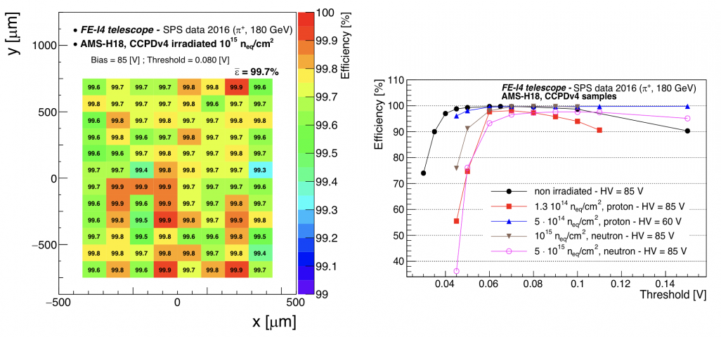 (Left) Particle detection efficiency measured at the CERN SPS test beam for a HV-CMOS CCPDv4 sensor irradiated with a fluence of 1∙1015 neq/cm2. The mean hit efficiency is measured to be 99.7%. (Right) Hit efficiencies as a function of threshold for different neutron and proton fluence. The drop in efficiency at 1.3∙1014 neq/cm2 is explained by the initial onset of trapping at these low fluences, as observed precedently [JINST 11 (2016) P04007].
The irradiated assemblies gave also excellent results. Hit efficiencies of 99.7% were measured for fluences of 1x10¹⁵ neq/cm2 as shown in the left figure above [arXiv:1611.02669, submitted to JINST]. Even at the extreme fluences of 5x10¹⁵ neq/cm2, hits efficiency was above 97% (see figure right).
After the very encouraging results obtained with these small sensors, we produced a full size (24.4×18.5mm2) HV-CMOS prototype in the less expensive ams-h350 process. The aim of this sensor was to demonstrate the feasibility of large area sensors using HV-CMOS technology that match in size the FEI4 chip. This large-area sensor (H35DEMO) [JINST 11 (2016) 01, C01012] was submitted to ams in October 2015 and produced in four different substrate resistivity (from 20 to 1000 Ω·cm). The sensor was delivered in February 2016. The IV-tests we performed in the clean rooms of the DPNC showed a breakdown above 160V. To characterise this full-size demonstrator w.r.t. radiation, we sent ten H35DEMO chips to the Ljubljana reactor to be irradiated with neutrons up to 1016 neq/cm2 and ten were irradiated up to similar doses with proton at the Bern cyclotron. Laboratory and beam tests have shown that the H35DEMO works perfectly and provides the same excellent efficiency measured with the CCPDv4 sensor.
A first monolithic ams chip, named ATLASPix1, was submitted early in 2017 in the ams-aH18 technology. This new technology allows for the test of fully isolated CMOS circuitry that was recently implemented by ams for our needs. The first testbeam results (October 2017) obtained with the CLICdp Timepix3 telescope for a 80 Ωcm substrate resistivity chip operated at a threshold of ~2000 electrons, shows a uniform efficiency larger than 99.5%.
Group contributors:
Giuseppe Iacobucci, Mathieu Benoit, Winnie Wong, Sergio Gonzales-Sevilla, D.M.S. Sultan, Didier Ferrére, Stéphane Debieux, Daniel la Marra, Yannick Favre, Ettore Zaffaroni
Former members: Alessandro La Rosa, Daniel Muenstermann, Fadoua Guezzi-Messaoud, Javier Bilbao de Mendizabal (thesis), Lingxin Meng (thesis), Antonello Miucci (thesis), Branislav Ristic (thesis), Francesco Di Bello (thesis), Mateus Vicente-Barreto-Pinto (thesis), Le Li (thesis)
Collaborating Institutes:
Argonne National Laboratories, LHEP Bern University, Brookhaven National Laboratories, CERN, Heidelberg University, IFAE Barcelona, Karlsruhe Institute of Technology, Liverpool University, Tsukuba University
Supported by:
Selected Publications
-
Test results of ATLASPIX3 – A reticle size HVCMOS pixel sensor designed for construction of multi chip modules
Schimassek R. et al.
NIMA 986 (164812) (2020)
-
A data acquisition system for HV-CMOS sensor research and development in the upgrade of ATLAS experiment
K. CHEN et al.
Review of Scientific Instruments (2019) 90 (064701) (2019) -
Characterisation of AMS H35 HV-CMOS monolithic active pixel sensor prototypes for HEP applications
Terzo S. et al.
JINST 14 P02016 (2019) -
Development of FELIX based readout system for HV-CMOS sensor testbeam
W. WU et al.
JHEP 14 (1) P01013 (2019)
-
Test beam measurement of ams H35 HV-CMOS capacitively coupled pixel sensor prototypes with high-resistivity substrate
Benoit M. et al.
JINST 13 P12009 (2018) -
Charge collection characterisation with the Transient Current Technique of the ams H35DEMO CMOS detector after proton irradiation
J. ANDERS et al.
JINST 13 (P10004) (2018) [arXiv] -
Testbeam results of irradiated ams H18 HV-CMOS pixel sensor prototypes
M. Benoit et al.
JINST 13 (P02011) (2018) [arXiv]
-
Testbeam results of irradiated ams H18 HV-CMOS pixel sensor prototypes
M. BENOIT et al.
JINST 13 (P02011) (2017) [arXiv] -
Development of a modular test system for the silicon sensor R&D of the ATLAS Upgrade
H. LIU et al.
JINST 12 P01008 (2017) [arXiv]
-
Results of the 2015 testbeam of a 180 nm AMS High-Voltage CMOS sensor prototype
M. BENOIT et al.
JINST 11 P07019 (2016) [arXiv] -
The FE-I4 Telescope for particle tracking in testbeam experiments
M. BENOIT et al.
JINST 11 P07003 (2016) [arXiv] -
Prototyping of an HV-CMOS demonstrator for the High Luminosity-LHC upgrade
E. VILELLA et al.
JINST 11 (C01012) (2016) [Other link]