
IDE interface card prototype
A fine mess o' wires, isn't it? And yet it works!
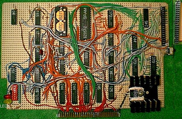
PE-box connector
Connections #2 to 60 on this side, connections #1 to 59 on back
side
(small PCB glued to the prototyping board).
244: three 8-bit buffers, 74LS244 for the address bus and
control
lines (74LS245 would also do).
245: A 8-bit transceiver, 74LS245 for the data bus.
125: A quad 74LS125 buffers, for 3-state output signals
(RDBENA*
and EXTINT*).
7805: A voltage regulator, 7805CT, +5 volts, 1 Amp. A 22 uF
cap is located under then lower part of the heat sink.
CRU logic
85: A 4-bit comparator, 74LS85 to compare the CRU address to
that set on the DIP-switch.
DIP: Dual-in-line 7-switch package (only 5 are used). Note
the
blue 4.7K pull-up resistor network.
259: An 8-bit addressable latch, 74LS259 for CRU output
operations
251: An 8-to-1 multiplexer, 74LS251 for CRU input operations
(unbuffered CRUIN line to the PE-box).
LEDs: A yellow light-emitting diode reacts to CRU bit 0, a
red
one to IDE access. A 270 ohm resistor for each.
Address selection logic
138: A 3-to-8 decoder, 74LS138 does most of the work.
688: An 8-bit comparator, 74LS688 to detect the register
mapping
area (>4000-40FF).
139: Half a dual 2-to-4 decoder, to select among the
devices:
clock / SRAM / IDE port1 / port3
Sw: Main switch. Prevents the card to answer to CRU
commands,
hence to memory operations (which need bit 0).
Static RAM
628512: A 512 kbytes SRAM, HM628512ALP-5 to store the DSRs
and
the file buffers (upside-down).
373: An 8-bit latch, 74LS373, to store a page number for the
SRAM.
Eight 4.7K pull-down resistors, to select page 0 when the '373 is
in
high impedance state.
Clock
A RTC65271 real-time clock, with 4 Kbytes of SRAM and an
on-chip
crystal (upside-down).
Two +3 volts, BR1225 batteries in an on-chip battery holder.
Bus demultiplexer (8 <=>16 bits)
139: Half a dual 2-to-4 decoder to decode read/write on
odd/even
bytes operations.
244: An 8-bit buffer, to read odd bytes from the IDE ports.
373: Two 8-bit latch, 74LS373, to latch odd bytes upon
writing
and even bytes upon reading.
245: An 8-bit transceiver, to write the even byte to IDE
ports
(historical reasons: should be a 74LS244).
IDE connector: pins # 1 and 40 indicated. Pin #20
(key)
removed to prevent wrong connections.
Insert: IDE cable, to connect two drives. Hole #20 plugged
to
prevent upside-down connections.
Pulse generator
165: A 74LS165 shift registers produces WR* and RD* pulses
for
the IDE controller.
Logic gates (used in parts by the above sections)
32: Two quad OR gates, 74LS32.
02: A quad NOR gates, 74LS02.
08: A quad AND gates, 74LS08.
04: Two hex inverters, 74LS04.
Note the tiny yellow bypass cap (100 nF) above each chip
Color code
Red: unbuffered signals
Orange: address bus.
Orange/white:
signals derived from address lines.
Green: 8-bit data bus.
Green/white:
least significant byte in 16-bit bus.
Blue: CRU bit lines.
Blue/white:
signals derived from CRU bits.
Brown: Control lines (RDBIN,
MEMEN*,
etc). Brown/white: signals derived from control lines.
Black: power lines
Revision 1. 5/24/00. Preliminary, not for release.
Revision 2. 8/26/01. New dempx, pulse generator. OK to release.
Back to the TI-99/4A Tech Pages.