
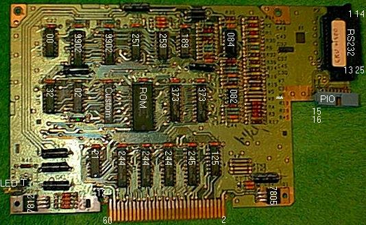
RS232c / PIO interface card
* This card was modified so as to
answer
at CRU >1500. This lets me have two RS232 cards in my PE-box. See below
for details.
PE-box connector
Connections #2 to 60 on this side, connections #1 to 59 on back side
244: Three 8-bit buffers, 74LS244 for the address bus and
control
lines.
245: A 8-bit transceiver, 74LS245 for the data bus.
125: A quad 74LS125 buffers, for 3-state output signals
(e.g.
RDBENA* , EXTINT*).
7805: Voltage regulator, TL780-05C, +5 volts. Three 47 uF
bypass
caps (C12, C40, C41).
7812: Voltage regulator, 78M12C, +12 volts. Two 47 uF bypass
caps (C13, C38).
-12: Negative voltage regulator, 79L12A. Two 47 uF bypass
caps
(C18, C100).
CRU logic
259:An 8-bit addressable latch, 74LS259 for CRU output.
251: An 8-to-1 multiplexer, 74LS251 for CRU input operations
(unbuffered CRUIN line to the PE-box).
T: A transistor NP2N3904 to control the LED.
LED: A yellow light-emitting diode controlled by CRU bit 7
(not
bit 0 as usual!).
Memory
ROM: A 4K ROM, labelled CD3235A-NL DBT8240
Selection logic
Custom: Custom control chip, labelled I500280-3 RS00MMI8245.
Selects the ROM (pin #13), the PIO port (pin # 14 for PIO in, pin #15
for
PIO out), CRU chips (pin #16), and TMS9902 chips (pin #17 for RS232/1,
pin #18 for RS232/2).
00: A quad NAND gates, 74LS00. One gate not used.
02: A quad NOR gates, 74LS02.
21: A dual 4-input AND gates, 74LS21.
32: A quad OR gates, 74LS32.
PIO port
373: Two 8-bit latches, 73LS373. One for input, one for
output.
PIO: Parallel port connector, 16 pin. Odd pins on top, even
pins at bottom.
RS232c port
9902: Two UART chips, TMS9902. Each handles one serial port.
084: A TL084ACN quad op amp, -12 to +12 volts. Handles TX
and
DCD output lines.
082: A TL082CP dual op amp, -12 to +12 volts. Handles CTS
output
lines.
189: A 75189 quad inverters. Handles RD and DTR input lines.
RS232: DB-25 connector combining the two RS232C ports in a
single
plug. Pin 1 to 12 on top, 14 to 25 at bottom.
CRU modification
This card is designed so that two cards can be installed in the
PE-box,
one with CRU >1300, the other with CRU >1500. The DSRs are
written
so as to handle this situation and provide two parallel ports and four
serial ports.
Unfortunately, instead of using a simple switch, TI designed the
card
so that a resistor must be moved to change the CRU. This resistor is
identified
as R5 (see the green star * in the
picture
above) and must be moved in the position labelled PTH1 (just below it).
Here is a blow-up of the modification:
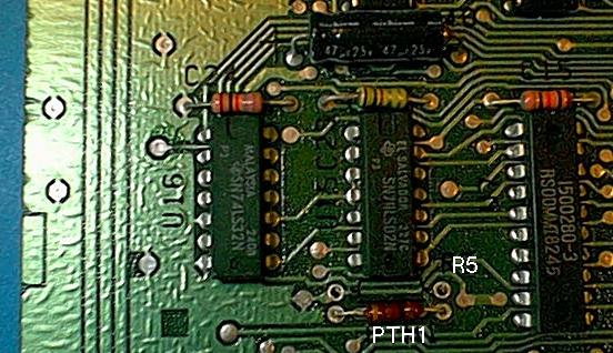
The resistor was initially in position R5, just below the 74LS02. I
desoldered it and transplanted it to position PTH1. This connects pin19
of the custom control chip (on the right of the picture) to +5 volts,
instead
of ground.
Pin assignment modifications
TI also made provisions for us to change the pin assignments for the
DTR lines. Normally DTR-1 is pin 20 (jumper W5) and DTR-2 is pin 19
(jumper
W6). However, It is possible to assign DTR-1 to pin 11 instead, by
cutting
W5 and replacing it with a jumper at W7. Similarly, DTR-2 can be
assigned
to pin 18 by cutting W6 and wiring W8.
The location of these jumpers is flagged by two white stards ** on
the
main picture. Note that jumper W7 is a bit further up.
The above card was not modified in such a way, as I'm not sure what
this modification is meant for.
For further details, see my RS232c page.
Revision 1. 8/26/01. OK to release.
Back to the TI-99/4A Tech Pages