Several solutions have been though of to overcome this problem: drawing an extra cable to carry the remaining 8 bits, multiplexing them with the address bus instead, etc. Recently, it occured to me that memory and TTL chips are so fast, that it probably wouldn't be necessary to have 4 wait states. I started studying the wait-state generator in the console, and found that it could easily be modified so that the number of wait states can be controlled by software: 4, 3, 2, 1... or even 0 !
Software-control is important since some peripherals may not like a faster multiplexer, and some programs containing delay loops may be thrown off by the increase in speed. For instance, the Floppy Disk Controller ROMs contains several loops waiting for the drive to be ready. Speeding up execution may cause these loops to time out too early and report a faulty drive. In such cases, you would select the normal 4-wait-states multiplexing. But you still have the ability to speed up your favorite programs!
Hardware description
Instructions timing
The wait state generator
The WE* pulse generator
About clock signals
Hardware modifications
Removing two wait states
_Timing diagram
_Doing it
_Testing it
Down to one wait state
_Timing diagram
_Doing it
Zero-wait-states
_Timing diagram
_Write/Acquire problem
_GROM issues
_Doing it
_Testing it
All-or-none version
Finding CRU bits
Software control
       AORG >8300           Program loaded in fast memory
*      LWPI >83E0           Assume workspace is also in fast memory
HERE   MOV  @>2000,R0     } Our loop
       JMP  HERE          }
This loop requires a total of 36 memory cycles (marked below by Phi3*), and consists in 11 main operations:
 | | | | | | | | | | | | | | | | | | | | | | | | | | | | | | | | | | | |  Phi3*
  1       2 ____  3   4       5       6   7   8_  9  10         11
|___|   :...:   |___|   |___________|   |___|   |_______|               | Memen*
_________________________________________________    ___________________
 ___                                             |__|___                  WE*
|MOV|_______________________________________________|JMP|_______________  IAQ
 ___             ___     ____            ___     _______
|   |___________|   |___|    |__________|   |___|       |_______________  A15/CruOut
  a       c       a   c   a     a   | c   a   c   a | a         c
1) 2 cycles. Fetch the first program word (MOV, with type of operands and register numbers)
a) A15/CruOut reflects A15 (which is high, when not in use).
c) A15/CruOut reflects CruOut (which is low, when not in use).
For simplicity, the above program was loaded into the scratch-pad memory, which is quite unusual. Normally, it would reside in the memory expansion, so points (1), (3) and (10) would also have an extra 4 wait cycles in them. Similarly, if the workspace were not in the scratch-pad, points (7) and (9) would require an extra four wait cycles. This would bring the total number of cycles to 56, from a theoretical minimum of 32.
Note that although memory access is three times slower in the PE-box, most programs will only be about twice slower. This is because every instruction comprises many the internal computation cycles, that are not affected by wait states. In addition, if the programmer was smart enough to place his workspace and his most frequently used variables in the scratch-pad, you will only gain speed when the processor is reading the program itself from 8-bit memory. But even this is quite appreciable.
Now you see why wait states are a drag. But how are they generated?
| 74LS04 WE*|-----------------------------------------------------------|>o----, | ,------------------, | | 74LS00 ,---o(|=---, ,---+5V | 74LS74(A) | | '04 ,----o(|=----, '-o(|=--, | +------+ | READY|--o<|---o(|=--, | +-------+ | | Phi4*-|Ck | | -------+ | +---|Clr* QA|--' | | | | TMS9900 | '04 | | QB|----------|-------|Pr* | | '00 +------+ | ,--|>o-' | QC|----------+-------|D Q|--=|)o--WE* Phi2*---|Ck Q|------+---|----------|S0 QD| '04 | +5V---|Clr* | | | +----------|S1 Sr|--+--o<|--' +------+ SysRdy--|D | | Phi1*---|Ck | '-------------------------------A15 | | Start*--' Gnd---|A Sl| +5V---|Clr* | Gnd---|B | +5V---|Pr* | Gnd---|C | +------+ |D | 74LS194 74LS74(B) +-------+ |
The heart of the generator is the 74LS194 universal shift register. This register is controlled by a signal called "Start*". This signal is normally high, but becomes low during a memory operation (Memen* low) that does not access the console ROMs (addresses >0000-1FFF), nor the console RAM pad (addresses >8000-83FF). When Start* is high, it inhibits the 74LS194 via its Clr* input, after being inverted by a 74LS04. It also presents the S1 input with a high level, which puts the 74LS194 in "parallel load" mode, i.e. inputs A through D are latched for futur output. Note that the inverted Start also inhibits any wait signal generated by the 74LS194 from reaching the CPU, by masking them with a NAND gate.
On the other hand, wait requests coming from elsewhere (such as from the GROMs) do reach the TMS9900. This signal is labelled SysRdy in the above schematics. It is latched by a 74LS74 clocked by Phi2*, although this may seem irrelevant since the TMS9900 only samples its Ready pin during Phi1. So why the 74LS74? It's here to synchronize this external signal with the 74LS194, in case a memory chip requests even more wait states than the generator is creating. Pulling low the S0 input when the 74LS194 is active, results in a hold state (S0=0, S1=0) that will begin and end on a Phi2* rising edge. Once the memory chip is ready to go on, the 74LS194 resumes counting wait states where it stopped.
When Start* is active (low), the 74LS194 is enabled and placed in the "shift-to-the-right" mode. Each low-to-high transition on Phi1* (i.e. its trailing edge) will transfer QA to QB, QB to QC, etc. Note that D and QD are not used in this circuit and can thus be ignore.
Also note that the output QC is inverted to make up the extra address line A15. By convention, A15 must be high first to transfer the odd-numbered data byte, then low to transfer the even byte. The A15 signal is also applied to the serial-right input SR of the 74LS194, which means that it will appear in QA at each shift operation. In summary, every time Phi1* goes high, we have: QC = QB, QB = QA, QA = -QC.
Initially, all inputs are low since they were reset by Clr*. Which gives us the following sequence of event:
QA QB QC
L  L  L  Initial state. A15 is high.
H  L  L
H  H  L
H  H  H  A15 toggles here
L  H  H
L  L  H  etc
Several NAND gates combine these outputs to generate the wait signal. A wait state occurs when QC is low, or when QA is high. In the above table, this occurs for the first four lines, so each of these cycles will be followed with a wait cycle. The first and last lines are the regular memory cycles:
QA QB QC  Wait? Cycle
L  L  L   w     Regular
H  L  L   W+w   Wait
H  H  L   W+w   Wait
H  H  H   W     Wait (A15 toggles here)
L  H  H         Wait
L  L  H         Regular, end of operation
W indicates a wait signal due to QC being low.
w indicates a wait signal due to QA being high.
Wait signals cause the next cycle to be a wait state.
The following is a timing diagram for a regular memory cycle (e.g. accessing the console ROMs). Note that it's not drawn to scale.
_           W           W
 |_________| |_________| |_________  Phi1
   _       |   _       |   _
__| |______|__| |______|__| |_______ Phi2
  |   _    |      _    |  |   _
__|__| |___|_____| |___|__|__| |____ Phi3
  |      _ |         _ |  |      _
__|_____| ||________| ||__|_____| |_ Phi4
__|        |           |  | ________
  \________|___________|__|/         MEMEN*
___________|           | ___________
           \___________|/            WE*
The cycle begins on the leading edge of Phi2 (Memen* goes low) and ends two cycles later, also on the leading edge of Phi2. For read operations, the TMS9900 would input data during the last Phi1. For write operations, the WE* pulse becomes active (low) on the leading edge of the first Phi1 and end on the leading edge of the next Phi1.
The wait signal is sampled during the first Phi1 pulse (marked W), and wait cycles will be added from Phi2 to Phi2 if requested.
This means that the WE* line is going to remain low during the whole multiplexing process. This is not what we want: we need two WE* pulses, one when A15 is high to latch the odd byte, then one when A15 is low, to latch the even byte.
This is achieved by the second half of the 74LS74 in the above schematic: it is clocked by Phi4*, preset by QB low and it latches QC. When QB is high and QC is low, the next rising (i.e. trailing) edge of Phi4* will cause the output Q to go low. This output is combined with an inverted WE* to provide a new WE* signal. When Q is high, the output is determined by WE*, but when Q is low, the output is always high. In essence, Q serves to mask WE* during one clock cycle, from Phi4* to Phi4*.
If you look at the cycle table above, you will notice that the only moment when QB is high and QC low is just before A15 toggles. Thus, the WE* line will become high while A15 toggles, then low again. Two pulses, just like we wanted!
Here is what the timing diagram for 4 wait states looks like:
_       _       _       _       _       _       _
 |_____|w|_____|w|_____|w|_____|W|_____| |_____| |_____ Phi1
  _       _       _       _       _       _       _
_| |_____| |_____| |_____| |_____| |_____| |_____| |___ Phi2
    _       _       _       _       _       _       _
___| |_____| |_____| |_____| |_____| |_____| |_____| |_ Phi3
      _       _       _       _       _       _       _
_____| |_____| |_____| |_____| |_____| |_____| |_____|  Phi4
__                                                 ____
  \_______________________________________________/     MEMEN*
________                                         ______
        \_______________________________________/       WE* (cpu)
           _______________________
__________/                       \____________________ QA 74LS914
                   _______________________
__________________/                       \____________ QB
                           _______________________
__________________________/                       \____ QC
__________________________                         ____
                          \_______________________/     A15
________________________         ______________________
                        \_______/                       Q 74LS74
________                 _______                 ______
        \_______________/       \_______________/       WE* (PE-box)
            ~666 ns                  ~666 ns
Note that each WE* pulse lasts from Phi1 to Phi1, just like a non-multiplexed pulse. Which was probably the reason for inserting 4 wait states, in the first place.
The TIM9904 generates four such pulses, in successive phases, each a quarter of a cycle (83 ns) apart. These are called Phi1, Phi2, Phi3 and Phi4 and are meant for use by the TMS9900 microprocessor. If you do the math (12+45+12 vs 83) you will notice that there is a short gap between the end of one pulse and the beginning of the next. This can be seen in the first timing diagram above, but I omitted it from subsequent diagrams, for the sake of clarity.
The TIM9904 also generates TTL-compatible signals, to be used by the on-board circuitery. These signals are mirror image of the above ones, i.e. they are active low. They are named Phi1*, Phi2*, Phi3* and Phi4* (by convention, a * denotes an active-low signal).
Most events are triggered when a clock signal goes from low to high, so TMS9900 internal events generally occur on the leading edge of a Phi pulse, whereas the cicuitery in the motherboard reacts to the trailing edge of a Phi* pulse.
The second modification is just as easy. It builds up on the first one and lets you remove a third wait state (#2) by adding an extra chip to the console: a cheap and easy-to-find 74LS74 TTL chip.
The third modification implies adding yet another cheap TTL chip to the console: a 74LS08 quad-AND gates. It builds up on the second one and lets you remove all four wait states, each under the control of a different CRU bit.
Finally, I'm suggesting a variant on this last modification, in which all wait states are controlled be the same CRU bit. You have less control on the number of wait states (basically, it's all or none), but you only need one CRU output.
If you prefer to control the wait states independently, you will need four CRU outputs. They can be taken from the TMS9901 chip, or by adding an extra CRU interface into the console.
If you don't know how to solder, don't panic: anyone can do it. Have a look at my howto page for a crash course in soldering.
Two-wait-states
One-wait-state
Zero-wait-states
All-or-none
Finding CRU outputs
These tools are described in more details in my howto
page. The page also suggests a few places where you can buy or mail
order this stuff.
There is one little problem though: the Clr* input of the 74LS194 overrides all other operations and holds all outputs low. This means that the inputs A through D won't be considered until Clr* becomes high. But when this happens, the Start* signal also switches the 74LS194 from "parallel load" mode to "shift right" mode. So when the next clock signal arrives, it will shift bits, not load them. In other words, input A though D are not taken into account!
Fortunately, this is easy to correct: we'll just hardwire Clr* high. We don't need this signal anyhow, since Start* can control shifting through the S1 input and mask out wait states through a dedicated NAND gate. The only thing we have to be carefull with, is that the external wait states act upon S0 and could place the 74LS194 in "shift-left" mode when Start* is inactive. So to be on the safe side, we'll just ground inputs D and SL (serial input left). This way, left shifts will keep the outputs low.
Note however, that this trick only lets us get rid of the wait states
issued before A15 toggles. Afterwards, the one remaining wait state
depends on QA being high, which is unavoidable after A15 went low. To get
rid of this last wait state we'll need to mask it out somewhere outside
the 74LS194. Fortunately this turns out to be very easy: instead of inverting
QA with a NOT gate (of which there are several spares in the console),
TI engineers used a NAND gate with the other input wired high. To stop
the wait signal at the level of this gate, all we need to do is to bring
this input low. It almost looks like they were planing for it...
TMS9900| 74LS04 WE*|---------------------------------------------------------|>o--------------, | ,---------------, | | ,-------' ,--Blk8* | | | 74LS00 ,-----o(|=-, ,-o(|=---Bit1 | 74LS74(A) | | '04 ,----o(|=---, '---o(|=------, | +------+ | READY|---o<|---o(|=--, | +-------+ | | Phi4*-|Ck Q*| | -------+ | | +5V--|Clr* QA|-' | | | | | '04 | | QB|----------|-------|Pr* | | '00 +------+ | ,--|>o-' | QC|----------+-------|D Q|--=|)o--WE* Phi2*--|Ck Q|------+--|------------------|S0 QD| '04 | +5V---|Clr* | | Q*| +------------------|S1 SR|--+--o<|--' +------+ SysRdy--|D | | Phi1*---|Ck | '----------------------------A15 | | Start*--' Bit2---|A | +5V---|Clr* | Gnd---|B SL|---Gnd red = modified +5V---|Pr* | Gnd---|C | +------+ Gnd---|D | 74LS74(B) +-------+ 74LS194 |
In summary, we now have two control points that can be programmed via CRU bits: the second input of the NAND gate (controlled by Bit1 and Blk8* in the above schematics) and the A input of the 74LS194 ( controlled by Bit2). Each removes one wait state in the second and first part of the memory cycle, respectively. Note that Bit 1 is active high and must therefore be inverted if you want your console to boot normally, with 4 wait states. This is achieved by using a spare gate left on a 74LS00 quad-NAND chip that's in the console.
So what's the Blk8* signal? You see, removing wait state #4 has an infortunate result: any wait request coming from the GROMs arrives too late to be taken into account by the CPU! Since GROMs need an awfull lot of wait states, the won't answer properly under these conditions. One way around this is through software: just make sure to enable wait state #4 prior to any GROM operation. But here I'm doing it with hardware: Blk8* is a signal present in the console, which is active (low) for memory operations in the range >8000-8FFF. I'm using this signal to mask out Bit1 and make sure wait state #4 will always be enabled when accessing GROMs, VDP, speech and sound chips. More on this later.
Here is the what the cycles will look like when removing the first wait state by setting the 74LS194 input A high:
QA QB QC  Wait? Cycle
H  L  L   W+w   Regular
H  H  L   W+w   Wait   }
H  H  H   W     Wait   } 3 wait states
L  H  H         Wait   }
L  L  H         Regular, end.
And here, when removing the last wait state by disabling the NAND
gate:
QA QB QC  Wait? Cycle
L  L  L   w     Regular
H  L  L   w     Wait   }
H  H  L   w     Wait   } 3 wait states
H  H  H         Wait   }
L  H  H         Regular, end.
Note the difference between the soutions: the first one removes
a wait state from the odd-numbered byte access (QC low, A15 high), whereas
the second removes it from the even-numbered byte access (QC high).
Now, if we combine the two, we get a two-wait-states memory access, with two clock cycles for the odd byte and two for the even byte:
QA QB QC  Wait? Cycle
H  L  L   w     Regular
H  H  L   w     Wait  }
H  H  H         Wait  } 2 wait states
L  H  H         Regular, end.
_       _       _       _       _       _
 |_____|w|_____|w|_____| |_____| |_____| | Phi1
  _       _       _       _       _
_| |_____| |_____| |_____| |_____| |_____  Phi2
    _       _       _       _       _
___| |_____| |_____| |_____| |_____| |___  Phi3
      _       _       _       _       _
_____| |_____| |_____| |_____| |_____| |_  Phi4
__                                 ______
  \_______________________________/        MEMEN*
________                         ________
        \_______________________/          WE* (cpu)
    ______________
___/              \______________________  QA 74LS914
           _______________________
__________/                       \______  QB
                   ______________________
__________________/                      \ QC
__________________
                  \________________1)____/ A15
________________         ________________
                \_______/                  Q 74LS74(A)
________         _______         ________
        \_______/       \_______/          WE* (PE-box)
         ~330 ns          ~330 ns
1) Note that we have introduced a permanent modification: A15 stays low at the end of the cycle, until the end of the next Phi1 pulse (~250ns). This should not bare any consequences, but will be corrected below when changing the clock inputs for the 1-wait-state modification..
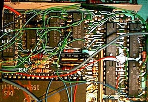
Locate the 74LS194 and the nearby 74LS00. They are just besides the clock chip. Here's a picture for you. And here's an ASCII diagram detailing the modifications to be done:
             ,-----------,
   +-,_,-+   |  +-,_,-+  |   +-,_,-+      +-,_,-+
   |     |   '--|1  16|]-'   |     |   ,--|1    |
   |     |      |     |      |     |   |  |     |
   |     |Bit2--|3    |      |     |   |  |     |
   |     |      |     |      |     |   |  |     |
   |     |      |     |      |     |   |  |   10|---Blk8*
   |     |   ,-[|6    |      |     |   |  |    9|---Bit1
   |     |   +-[|7    |      |     |   |  |    8|]-,
   |     |   '-[|8    |      +-----+   |  +-----+  |
   |     |      +-----+      74LS74    |  74LS00   |
   |     |      74LS194                '-----------'
   +-----+
   74LS362                --| : Cut pin                 TMS9901
   = 9904                 -[| : Intact pin              is over
-----------------------------------------------------+   there
            TMS 9900  microprocessor                 |     |
                                                     |     V
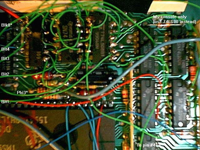
This is where to find the Blk8* signal:
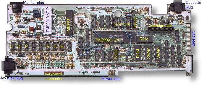
    __
 __|  |
|     |__________________________________________
|       74LS04      74LS03
|       +-,_,-+     +-,_,-+      +--------------+
|       |     |     |     |      |             ,|
|       |     |     |     |      | 74LS32      '|
|       |     |     |     |      +--------------+
|       |     |     |     |     +-,_,-+
|       |     |     |     |     |     |
|       |     |     |     |     |     |
|       |     |     |     |     |     |
|       +-----+     +-----+     |     |
|       +-,_,-+     +-,_,-+     |     |
|       |     |     |     |     | 74  |
\___    |     |Blk8*|     |     | LS  |
 ___|   |     |   | |     |     | 367 |
|===    |     |   | |     |     +-----+
|===    |     |   | |     |     +-,_,-+
|===    |   11|]--' |     |     |     |
|===    |     |     |     |     |     |
|===    |     |     |     |     |     |
|===    +-----+     +-----+     |     |
|===    74  +-,_,-+ 74LS138     |     |
|===    LS  |     |             |     |
|===    138 |     |             |     |
|=== S      |     |             |     |
|=== I      |     |             +-----+
|=== D      |     |             74LS367
|=== E      |     |
|===        |     |
|=== P      |     |
|=== O      |     |
|=== R      |     |
|=== T      +-----+
|===        74LS244
|===
Now where can you find CRU outputs? If this is the only console modification that you are planning, the easiest is to make use of the two spare outputs of the TMS9901 (the 40-pin chip with no heat sink on it, the closest to the TMS9900. See below). Just be aware that, while both are low upon power-up, one is turned high by the console power-up routines. Another alternative is to install my console CRU modification. It will provide you with upto 64 CRU outputs, or 32 outputs and 32 inputs, as you like. See the dedicated page.
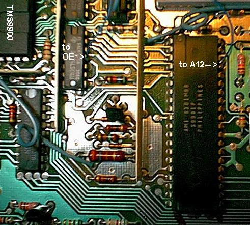
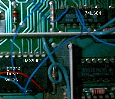
Assuming you decided to use the TMS9901, connect its pin #37 to the wire attached to the 74LS194, pin #3. Connect pin #38 to the wire attached to the 74LS00, pin #9. The TMS9901 pins need not to be cut, since they aren't connected to anything in the console. Here is a picture, in which pin #37 was used for a different modification, and is thus labelled "to A12". Pin #38 is just above it.
Note that the above wiring will suppress wait state #1 upon reset, as the console power-up routine always turns pin #37 high. By contrast, wait state #4 remains enabled. Alternatively, you could attach both wires to pin #38, but this means that you loose some of the fine control over wait states: it's either two or four, but never three...
And now, you can close your console. That's it, you made it!
To remove the first wait state, set CRU bit >0016 to one. To remove the last wait state, set CRU bit >0018 to one. Set them to zero to enable the corresponding wait states.
You will also need some kind of benchmark program, so you can measure the increase in speed.
Below is the result of my own testing. Note that, for my tests, I had a third wire placing input B of the 194 (pin #4) under the control of a CRU bit. This will be used later with the 1-wait-state modification. It wouldn't work right now because it prevents the first write pulse, but it was interesting for me to see if reading would work. Also, I didn't have Bit1 combined with Blk8* when I did those tests: it was coming straight from the CRU output. Later on I inverted it, then finally added an AND gate when I did the zero-wait-state modification. But of course an AND plus an inverter is the same as a NAND, which is why I told you to use the NAND gate.
This is somewhat strange, as the SRAM is enabled by a fairly simple circuitery after Memen* drops down: a 74LS138 decoder (in the console), and two 73LS32 OR gates (in the cartridge). All in all, a 50 ns delay at the most, whereas the odd-byte cycle is still about 666 ns in length.
I suspect that the problem may be due to the circuitery that holds high the CE* pin of the SRAMs when power is off, thanks to a +3V coin battery. This circuit comprises a capacitor connecting each CE* pin to +5 Volts. I don't know the capacitance of this component (labeled 221) but my guess is, it takes a long time for the last OR gate to issue enough current to charge the cap, and bring CE* low.
The card contains a complicated circuitery in charge of generating the RAS* (row address strobe) and CAS* pulses. Unfortunately, this circuit is clocked by Phi3* and is designed to count three clock cycles: RAS* is active during the first, CAS* during the next two. Then the cycle is repeated for the second byte (even address). In fact, it's repeated until Memen* goes high.
Not so surprisingly, when removing wait states the memory is not ready in time for a read: the odd byte (first accessed) reads as >FF, and the even byte actually returns the first byte.
The amazing thing is that write operations work all right, even with 3 wait-states removed! Even though removing a third wait state suppresses the write pulse, the card can still write the odd byte because it actually ignores the WE* line and uses only DBIN to tell reads from writes. But the strange thing is that the correct data gets written, instead of the previous byte, as with read operations. This may have to do with the fact that the 4116 chips need about 135 ns to read out data, whereas incoming data is latched in less than 55 ns after CAS* goes low...
Anyhow, the conclusion is that TI original 32K memory expansion card should only be used with all wait states enabled. By contrast, memory expansion boards based on SRAM (e.g. SuperAMS) should work flawlessly. I verified this with my IDE board: the 512K SRAM chip and the SRAM that's part of the clock chip both operate flowlessly with 2 wait states removed.
When performing a hard reset (power-on/off), the sound generator wouldn't shut up if wait state #4 was disabled by default. However, a soft reset (e.g. quit key) was no problem. Maybe this has to do with the time needed for the sound chip to power up???
Checking with a scope, I found out that removing wait state #4 prevents the GROMs from putting the CPU on hold altogether! Probably because the circuitery that generates the SysRdy signal is too slow. This is why I decided to mask Bit1 with the Blk8* signal. Note that I did it with an AND gate plus an inverter, but the NAND solution should work as well, if not better.
Under these conditions, the console boots all right and operates normally with two wait states removed.
To overcome this problem, an obvious solution is to rewire the half-74LS74 so that it is now clocked by Phi1* instead of Phi4*. This gives one clock pulse (~83 nanoseconds) for WE* to be low after we removed the first two wait states. But it also brings the end of WE* dangerously close to the point where A15 toggles, which could be a problem with peripherals that latch data on the trailing edge of WE*. So we'll have to also rewire the 74LS194, so that it is clocked by Phi2* instead of Phi1*. And of course, we should also rewire the second half-74LS74 so that the external SysRdy signal is clocked by Phi3* instead of Phi2*. In other words, we are going to delay all three components by one clock phase, i.e. 83 ns.
However, there is an extra difficulty: because the 74LS194 is enabled when Memen* goes low (on the leading edge of Phi2, followed by 6 TTL gates, which means a delay of about 60 ns), but is now clocked by the trailing edge of Phi2*, it will shift one more time, at the very beginning of the first clock cycle. This did not happen when it was clocked by Phi1*, because Phi1* occurs before Phi2.
The only solution I found to overcome this problem was to add an extra
chip inside the console: a simple 74LS74 dual-latch. Using one of the latches
we can delay the Start* signal so that it only toggles S1 at Phi4*. Since
Phi4* comes after Phi2*, we are back to the normal timing. Just to be on
the safe side, we will connect Start* to the Clr* input of the 74LS74,
so that it resets and freezes the latch as soon as Start* comes high (which
means that we must use the inverted Start signal, since Clr* is active
low). When Start* goes low, the latch is enabled, but will only toggle
at the next Phi4*. The D input is connected to +5V, but don't do it right
now because we will need to modify this later.
TMS9900| 74LS04 WE*|---------------------------------------------------------|>o--------------, | ,---------------, | | ,-------' ,--Blk8* | | | 74LS00 ,-----o(|=-, ,-o(|=---Bit1 | 74LS74(A) | | '04 ,----o(|=---, '---o(|=------, | +------+ | READY|---o<|---o(|=--, | +-------+ | | Phi1*-|Ck Q*| | -------+ | | +5V--|Clr* QA|-' | | | | | '04 | | QB|----------|-------|Pr* | | '00 +------+ | ,--|>o-+ | QC|----------+-------|D Q|--=|)o--WE* Phi3*--|Ck Q|------+--|------|-----------|S0 QD| '04 | +5V---|Clr* | | Q*| | | ,---------|S1 SR|--+--o<|--' +------+ SysRdy--|D | | | | Phi2*---|Ck | '----------------------------A15 | | Start*--' | | Bit2---|A | +5V---|Clr* | ,-----------' | Bit3---|B SL|---Gnd +5V---|Pr* | | | Gnd---|C | +------+ | +------+ | Gnd---|D | 74LS194 74LS74(B) '--|Clr* | | +-------+ Phi4*-|Ck Q*|---' +5V---|Pr* | | | new mod +5V---|D Q| 74LS74 (new) previous mod +------+ |
The new timing diagram, for 4 wait states, looks like this:
_       _       _       _       _       _       _
 |_____|w|_____|w|_____|w|_____|W|_____| |_____| |_____ Phi1
  _       _       _       _       _       _       _
_| |_____| |_____| |_____| |_____| |_____| |_____| |___ Phi2
    _       _       _       _       _       _       _
___| |_____| |_____| |_____| |_____| |_____| |_____| |_ Phi3
      _       _       _       _       _       _       _
_____| |_____| |_____| |_____| |_____| |_____| |_____|  Phi4
__                                                 ____
  \_______________________________________________/     MEMEN*
________                                         ______
        \_______________________________________/       WE* (cpu)

       ____________________________________________
______/                                            \___ Q* new 74LS74
             _______________________________
____________/                               \__________ QA 74LS914 (Phi2* clock)
                     _____________________________
____________________/                             \____ QB
                             _______________________
____________________________/                       \__ QC --> serial in
____________________________                         __
                            \_______________________/     A15
__________________________     ....____________________
                          \___:___/                     Q 74LS74(A) (Phi1* clock)
________                   _______               ______
        \_________________/   :...\_____________/       WE* (PE-box)
            ~749 ns                   ~583 ns
... = with 0-wait-states modificationOur rewiring has introduced the following permanent changes:
QA QB QC Wait? Cycle
H  H  L   W+w  Regular
H  H  H   W    Wait (A15 toggles here)
L  H  H        Wait
L  L  H        Regular, end
On top of this, we can also mask the last wait state with the NAND gate as before. The cycle table becomes:
QA QB QC Wait? Cycle
H  H  L   w    Regular
H  H  H        Wait (A15 toggles here)
L  H  H        Regular, end.
And we have achieved a one-wait-state cycle, with the following timing:
_       _       _       _
 |_____|w|_____| |_____| |_____ Phi1
  _       _       _       _
_| |_____| |_____| |_____| |___ Phi2
    _       _       _       _
___| |_____| |_____| |_____| |_ Phi3
      _       _       _       _
_____| |_____| |_____| |_____|  Phi4
__                         ____
  \_______________________/     MEMEN*
________                 ______
        \_______________/       WE* (cpu)
       ____________________
______/                    \___ Q* new 74LS74
____________________         __
                    \_______/   QA 74LS914 (Phi2* clock)
_______________________________
                                QB
             _____________
____________/             \____ QC
____________               ____
            \_____________/     A15
__________         ____________
          \_______/             Q 74LS74(A) (Phi1* clock)
________   _______       ______
        \_/       \_____/       WE* (PE-box)
       ~70 ns     ~250 ns
The WE* pulses are now quite short, especially the first one. For two-wait-states timing, we could either lengthen the first WE* pulse (to ~ 403 ns) by enabling wait state #2, or the second (to ~ 583 ns) by enabling wait state #4. With three wait states, we would lengthen both pulses.
 ,----------------------------------------,
 |    +-,_,-+       +-,_,-+       +-,_,-+ |      +-,_,-+
 |    |     |       |     |       |     | |      |     |
 |    |     |       |     |       |     | |      |     |
 |    |     |       |   14|- o  ,-|3    | |      |     |
 |    |     |  Bit3-|4    |     | |   11|-'o     |     |
 |    |     |       |     |     | |     |  |     |     |
 |    |     |       |   11|-,o--' |     |  |     |     |
 '---[|7    |       |     | |     |     |  |     |     |
      |     |       |     | |     +-----+  |     +-----+
      |     |       +-----+ |     74LS74   |     74LS00
      |     |       74LS194 '--------------'
      +-----+
      74LS362       ]-- : intact pin
      = 9904        |-- : cut pin
                    o-- : hole where pin was
-----------------------------------------------------+
            TMS 9900  microprocessor                 |
                                                     |
Here is a picture of this modification.
You will notice that at that time I hadn't thought of using Blk8* as a
masking signal. I was just inverting Bit1 with one of the spare gates on
the 74LS04: these are the wires that go to the right of the pictures. The
CRU bits come from the left because I'm using my console CRU interface
mod rather than the TMS9901. The wire labeled Bit2 is taped to the top
of the 74LS194, because I broke pin #3 when bending it out, so the soldering
is a bit fragile.
The second problem is that, in a no-wait-state cycle, the WE* pulse lasts one memory cycle: from Phi1 to Phi1. Which is also the duration of the masking pulse generated by the 74LS74! To mask only a portion of the WE* pulse, we need to make the masking pulse much shorter. Again, this will require an additional logic gate.
We will make use of a 74LS08 TTL chips, that comprises four independent AND gates. The schematics below shows how two of them should be installed. The first AND gate presets the 74LS74 when Phi4* goes low, effectively truncating its pulse. Remember that the 74LS194 and all clock inputs have been rewired as described above.
The second AND gate intercepts any wait signal coming from the 74LS194. Note that the CRU bit used (Bit4 here) is active high and thus needs to be inverted, since CRU bits are low upon power-up. Fortunately, there are several spare inverters in one of the 74LS04 present in the console, so we'll use one of them.
A third AND gate and a spare inverter found in a 74LS04 on the motherboard
are used to mask out Bit4 with the same Blk8* signals that we used with
Bit1. Again, this will prevent us from removing wait states when accessing
the memory-mapped devices: GROMs, VDP, etc. This is discussed in details
later.
TMS9900| 74LS04 (existing) 74LS04 WE*|---------------------------------------------------------|>o--------------, | ,--Blk8* | | ,o<|--(|=---Bit4 ,------------, | | 74LS08 (new) | ,----------' ,--Blk8* | | | 74LS00 ,-(|=-o(|=-, ,-o(|=---Bit1 | 74LS74(A) | | '04 ,----o(|=---, '---o(|=------, | +------+ | READY|---o<|---o(|=--, | +-------+ | Phi4* | Phi1*-|Ck Q*| | -------+ | | +5V--|Clr* QA|-' | | | | | | '04 | | QB|-----=|)--|-------|Pr* | | '00 +------+ | ,--|>o-+ | QC|----------+-------|D Q|--=|)o--WE* Phi3*--|Ck Q|------+--|------|-----------|S0 QD| '04 | +5V---|Clr* | | Q*| | | ,---------|S1 SR|--+--o<|--' +------+ SysRdy--|D | | | | Phi2*---|Ck | '----------------------------A15 | | Start*--' | | Bit2---|A | +5V---|Clr* | ,-----------' | Bit3---|B SL|---Gnd +5V---|Pr* | | | Gnd---|C | +------+ | +------+ | Gnd---|D | 74LS194 74LS74(B) '--|Clr* | | +-------+ Phi4*-|Ck Q*|---' +5V---|Pr* | | | new mod +5V---|D Q| previous mods +------+ 74LS74 |
_       _       _
 |_____| |_____| |_____ Phi1
  _       _       _
_| |_____| |_____| |___ Phi2
    _       _       _
___| |_____| |_____| |_ Phi3
      _       _       _
_____| |_____| |_____|  Phi4
__                 ____
  \_______________/     MEMEN*
________         ______
        \_______/       WE* (cpu)
       ____________
______/            \___ Q* new 74LS74
__________________
                  \____ QA 74LS914 (Phi2* clock)
_______________________
                        QB
             _____
____________/     \____ QC
____________       ____
            \_____/     A15
__________     ________
          \___/         Q 74LS74 (Phi1* clock, Phi4* enable)
________   __    ______
        \_/  \__/       WE* (PE-box)
      ~70 ns  ~83 ns
Again the WE* pulses are quite short, but there is no way around
since we must cram two pulses into the duration of one. Note however that
70 ns is a long time for a TTL or a memory chip. For instance, Flash-EEPROMs
protect themselves against spurious writing by disregarding overly short
pulses on WE* (e.g. statics). This noise cut off is set at 15 ns, so we
are well above this limit.
More critical is the fact the the second WE* pulse begins only ~140 ns after A15 toggled. Peripherals must decode the address and enable the data bus drivers before they can receive valid data and 140 ns may be a bit short, depending on the complexity of the decoding logic. However, assuming the peripheral has latched the first byte, the decoding circuit will already be active and the data bus enabled. Toggling A15 won't change a thing, so we should be all right. Problems may only occur with peripherals designed never to respond to odd-numbered bytes, but I don't think there are any.
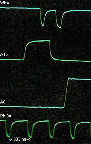
Here is a composite picture of signals captured by an oscilloscope during a write operation at @>2000, in zero-wait-state mode. A0 is provided as a mark for the end of the memory operation (Memen* stays low for the next operation). Phi3* is included to give you an idea of the time frame. Observe that the first write pulse indeed occurs while A15 is high (odd byte), the second when A15 is low (even byte).
Be aware that this modification of the masking pulse will also affect cycles in which the last wait state was not suppressed: the second WE* pulse will begin ~83 ns earlier than usual (i.e. when it used to start before we rewired the generator). But thanks to the wait state A15 has toggled ~250 ns earlier, so this sould be no problem, rather an advantage: it makes the second WE* pulse longer. This is illustrated with dotted lines in the 4-wait state diagram above.
But things are different when we are suppressing wait states: we now have less than 6 cycles per memory access and the last state may not always be L L H. So weird things start to happen, with A15 toggling at the wrong time, wait states being added or supressed, etc.
What we need to do is to cause the 74LS194 to reload (rather than reset) after a memory access is completed. That's easy enough to do: we must toggle its S1 input, which we can do by bringing low the D input of the 74LS74 that we added to the console. The only problem is to find a signal to trigger this action. We cannot use any of the outputs of the 74LS194, since their status will vary depending on the number of wait states we kept. So I decided to toggle S1 after two clock cycles that have no wait states. If you look at all the cycle tables in this page, you will find that they all end with two cycles that have no wait states.
This is best done with the other half of our piggy-backed 74LS74. The
two latches are wired as a flip-flop: each takes its input from the other,
but one of them inverts it, so each output will go L-H-L-H, etc. The second
latch is cleared by the Ready signal that goes low if there is any wait
states, which prevents toggling. When the Ready signal goes high (when
the 74LS194 shifts, at Phi2*), the 74LS74 is enabled, but it will only
toggle at the next Phi1*. In the mean time a Phi4* will occur, during which
the first latch will remain unchanged. Only after the second Phi4* will
the change appears on the S1 input of the 74LS194.
TMS9900| 74LS04 74LS04 WE*|---------------------------------------------------------|>o--------------, | ,--Blk8* | | ,o<|--(|=---Bit4 ,------------, | | 74LS08 | ,----------' ,--Blk8* | | | 74LS00 ,-(|=-o(|=-, ,-o(|=---Bit1 | 74LS74(A) | | '04 ,----o(|=---, '---o(|=------, | +------+ | READY|-+-o<|---o(|=--, | +-------+ | Phi4* | Phi1*-|Ck Q*| | -------+ | | | +5V--|Clr* QA|-' | | | | | ,--------' | '04 | | QB|-----=|)--|-------|Pr* | | '00 | +------+ | ,--|>o-+ | QC|----------+-------|D Q|--=|)o--WE* | Phi3*--|Ck Q|------+--|------|-----------|S0 QD| '04 | +5V---|Clr* | | | Q*| | | ,---------|S1 SR|--+--o<|--' +------+ |SysRdy--|D | | | | Phi2*---|Ck | '----------------------------A15 | | | Start*--' | | Bit2---|A | | +5V---|Clr* | ,-----------' | Bit3---|B SL|---Gnd | +5V---|Pr* | | | Gnd---|C | | +------+ | +------+ | Gnd---|D | 74LS194 | 74LS74(B) '--|Clr* | | +-------+ | Phi4*-|Ck Q*|---' | +------+ +5V---|Pr* | '--------|Clr* | | | this mod | Q*|-------|D Q|--, previous mods Phi1*--|Ck Q| +------+ | +5V---|Pr* | 74LS74(B) | | D|-----------------' +------+ 74LS74(A) |
In summary, this is what's hapenning when all wait states are disabled:
Time  74/Q*(B) Q*(A) 74LS194  Comments
Steady   H     H        =     Signal* is inactive
Phi2     H     H        =     Signal* becomes active
Phi2*    H     H      Load    S1 didn't see Signal* yet
Phi4*    L     H        =     Now it will
Phi1*    L     L        =     Toggles since no wait states
Phi2*    L     L      Shift   Second clock cycle
Phi4*    H     L        =     The 74LS74(B) toggles
Phi1*    H     H        =     The 74LS74(A) toggles
Phi2     H     H        =     Signal* becomes inactive, end
And with one wait state:
Time  74/Q*(B) Q*(A) 74LS194  Comments
Steady   H     H        =     Signal* is inactive
Phi2     H     H        =     Signal* becomes active, enables wait states
Phi2*    H     H      Load    Outputs a wait state for sure
Phi4*    L     H        =     The 74LS74(B) toggles
Phi1*    L     H        =     The 74LS74(A) is cleared by the wait state
Phi2*    L     H      Shift   Second clock cycle, no more wait states
Phi4*    L     H        =     No changes
Phi1*    L     L        =     Now 74LS74(A) can toggle
Phi2*    L     L      Shift   Third clock cycle
Phi4*    H     L        =     The 74LS74(B) toggles
Phi1*    H     H        =     The 74LS74(A) toggles
Phi2     H     H        =     Signal* becomes inactive, end
An additional benefit of this design is that it takes care of the
"shift-left" problem due to peripheral wait requests arriving when there
is no wait state. Since the Ready signal incorporates both types of wait
requests, peripheral requests (in this case latched at Phi3*) will immediately
reset the 74LS74, which at the next Phi4* will set the S1 input of the
74LS194 high, thereby insuring that it is in "hold" state (S0=0 S1=0) for
the next Phi2*.
Time  74/Q*(B) Q*(A) 74LS194  Comments
Steady   H     H        =     Signal* is inactive
Phi2     H     H        =     Signal* becomes active. Peripheral takes notice
Phi2*    H     H      Load    Sometime around now, it asks for a wait state
Phi3*    H     H        =     Peripheral wait request is latched
Phi4*    L     H        =     The 74LS74(B) toggles
Phi1*    L     H        =     The 74LS74(A) is frozen by the wait state
Phi2*    L     H      Hold    S0 low (by peripheral demand), S1 low by 74LS74(B)
Phi3*    L     H        =     Lets say the peripheral is now ready
Phi4*    L     H        =     No changes
Phi1*    L     L        =     Now 74LS74(A) can toggle
Phi2*    L     L      Shift   Back to normal cycles
Phi3*    L     L        =     No changes
Phi4*    H     L        =     The 74LS74(B) toggles
Phi1*    H     H        =     The 74LS74(A) toggles
Phi2     H     H        =     Signal* becomes inactive, end
So why multiplex these addresses? Most probably for timing questions. These devices, expecially the GROMs, are very slow and cannot answer within a regular 2-clock-cycle memory operation. So circuitery was added to the console so GROM access automatically triggers the SysRdy line and puts the CPU on hold until the GROMs are ready to answer, which can take over 24 clock cycles!
But there is a problem here: the cicuitery that generates this holding signal is fairly complex (two 74LS138, and two 74LS03). As a result, it takes time for SysRdy to go low after A15 has toggled. If we remove wait state #4, the request for a hold actually arrives too late for the CPU to take it into account. The situation is even worse with zero-wait-states timing, where there is no way the signal can get there in time.
So what to do? My solution was to mask out Bit1 and Bit4 with a signal, which I called Blk8*, taken from a 74LS138 in the console reacting to addresses >8000-8FFF. When such an address is accessed, wait states #3 and #4 are automatically enabled, regardless of the status of CRU bits 1 and 4. This lets us access the memory mapped devices with regular timing (except for wait states #1 and #2, but these affect the odd-numbered byte, which memory mapped devices ignore).
Bit4 is masked with an AND gate, from the piggy-backed chip, prior to being inverted. Bit1 could be masked the same way (actually that's what I did in my console), but we could also make use of the spare NAND gate left in the 74LS00. This is what I've described in the previous schematics. Since NAND is the same as AND plus NOT, the two solutions are equivalent.
For the 74LS08:
      +-,_,-+
     =|     |]
     =|     |=        [| : intact pin
     =|     |=        =| : bent & trimmed
     =|     |=
     =|   10|=-,
     =|     |=-+
   ,-[|     |= |
   |  +-----+  |
   |   74LS08  |
   '-----------'
And for the 74LS74
    ,-----------,
    |  +-,_,-+  |
    | =|   14|]-+
  ,-|-=|2    |= |        [| : intact pin
  | | =|   12|=-|-,      =| : bent & trimmed
  | '-=|4    |= | |
  |   =|   10|=-' |
  | ,-=|6   9|=-, |
  | | [|     |= | |
  | |  +-----+  | |
  | |   74LS74  | |
  '-|-----------' |
    '-------------'
            |
  +-,_,-+   |   +-,_,-+       +-,_,-+       +-,_,-+
  |     |   '-o |1    | |  |  |     |       |     |
  |     |       |     | |  |  |     |       |     |
  |     |       |   14|-'o-'  |     |       |     |
  |     |       |     |       |     |     | |     |
  |     |       |     |       |     |     | |     |
  |     |       |     |       |     | ,--o'-|6    |
  |     |       |   10|---,   |     | '--   |     |
  |     |       |     |   |   +-----+       +-----+
  |     |       +-----+       74LS74        74LS00
  |     |       74LS194
  +-----+                     --[| : intact pin
  74LS362                     ---| : cut pin
  = 9904                      ---o : hole where pin was
-------------------------------------------------+
        TMS 9900  microprocessor                 |
                                                 |
            ,--------------------------,
  +-,_,-+   |   +-,_,-+       +-,_,-+  |    +-,_,-+
  |     |   '-o |     |      =|1  14|] |    |     |
  |     |       |     |      =|   13|--'    |     |
  |     |       |   14|      [|3    |=      |     |
  |     |       |     |      =|     |=      |     |
  |     |       |     |      =|     |=      |     |
  |     |       |     |      =|     |=      |     |
  |     |       |   10|---,  [|7   8|=-,    |     |
  |     |       |     |   |   +-----+  |    +-----+
  |     |       +-----+   |   74LS74   |    74LS00
  |     |       74LS194   '------------'
  +-----+                       [| : solder to underlying pin
  74LS362                     ---| : cut pin
  = 9904                      ---o : hole where pin was
-------------------------------------------------+
        TMS 9900  microprocessor                 |
                                                 |
                        ,-----------------,
                        |   ,-----------, |
                        |,--|---------, | |
  +-,_,-+       +-,_,-+ ||  | +-,_,-+ | | | +-,_,-+
  |     |       |     | ||  | |     | | | '=|1    |]
  |     |       |     | ||  | |     | | +--=|2  13|=---Blk8*
  |     |       |   14|-'o  o |3    | '-|--=|3  12|=---Bit4
  |     |       |     |       |   11|=--'  =|     |=
  |     |       |     |       |     |      =|     |=
  |     |       |     |       |     |      =|     |=
  |     |       |     |       |     |      [|     |=
  |     |       |     |       +-----+       +-----+
  |     |       +-----+       74LS74        74LS08
  |     |       74LS194       on top of     on top of
  +-----+                     74LS74        74LS00
  74LS362          [ : solder to underlying pin
  = 9904         --| : cut pin    -=| : pin of top chip
                 --o : hole where pin used to be
-------------------------------------------------+
        TMS 9900  microprocessor                 |
                                                 |
                                          ,--------------------------,
  +-,_,-+       +-,_,-+       +-,_,-+     | +-,_,-+        74LS00    |  74LS00
  |     |       |     |    ,-=|1    |]    | |     |        +-,_,-+   |  +-,_,-+
  |     |       |     |    | =|     |=    | |     |        |     |   |  |     |
  |     |       |     |    | [|     |=    | |     |        |     |   |  |     |
  |     |       |     |    | =|     |=    '=|4  11|-----,  |     |   |  |     |
  |     |       |     |    | =|     |= ,---=|5    |     |  |     |   |  |     |
  |     |       |     |    | =|     |= | o-=|6    |     |  |     |   |  |     |
  |     |       |     |    | [|     |=      |     |     |  |     |   |  |     |
  |     |       |     |    |  +-----+       +-----+     |  |     |   |  |     |
  |     |       +-----+    |  74LS74        74LS08      |  +-----+   |  +-----+
  |     |       74LS194    |                on top of   |  +-,_,-+   |  +-,_,-+
  +-----+                  |                74LS00      |  |     |   |  |     |
  74LS362                  |   ___| : bottom chip       |  |     |   |  |     |
  = 9904                   |   --=| : top chip          |  |     |   |  |     |
                           '--------------------------, |  |     |   |  |     |
---------------------------------------------------+  | '------------|--|5    |
          TMS 9900  microprocessor                 |  |    |     |   '-[|6    |
                                                   |  |    |     |      |     |
                                                   |  |    +-----+      +-----+
                                                   |  |    74LS32       74LS04
                                                   |  |    +-,_,-+
                                                   |  |    |     |
---------------------------------------------------+  |    |     | <--74LS04
                                                      |    |     |
                                                      '----|4    |
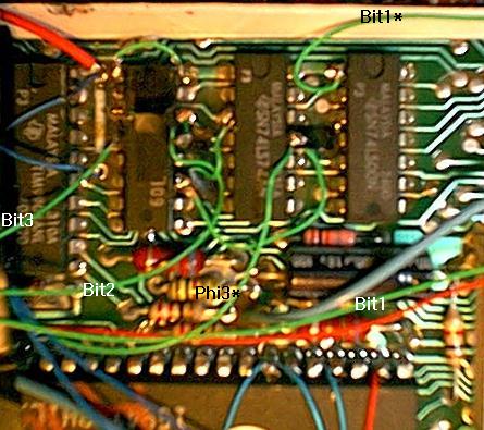
Here is a picture where only the 74LS08
was piggy-backed, and here is one where both chips
are in place. Only consider the green wires: the other colors correspond
to different modifications. Two of which are making use of the spare bits
on the TMS9901, so I had to implement an extra CRU interface in the console:
you may notice that the CRU bits come from the left. Also, for historical
reasons, I was not using the spare NAND gate, but rather the fourth AND
gate on the piggy-backed 74LS08, following with yet another spare inverter
on the 74LS04. The two circuits are equivalent. What's still missing here
is a piece of electrical tape, to make sure the pins of the piggy-backed
chips won't make contact with the metal shell around the motherboard.
Condition      Bit1 Bit2 Bit3 Bit4  Wait states
4 wait states   0    0    0    0     1 2 3 4
3 wait states   0    1    0    0     - 2 3 4
3 wait states   1    0    0    0     1 2 3 -
2 wait states   1    1    0    0     - 2 3 -
1 wait state    1    1    1    0     - - 3 -
0 wait states   x    1    1    1     - - - -
There are 9 additional combinations of bits, but these may yield weird results. For instance, 0 0 1 0 puts the computer in a forever waiting state (!). As a general rule, Bit3 should never be 1 unless Bit2 is also 1. And Bit4 should never be 1, unless both Bit2 and Bit3 are also 1.
You should run some kind of benchmark program to verify that the speed is actually increased. If you have "exotic" hardware, try and see if it can cope with the increase in speed. If not, try to figure out whether it's a hardware issue, or if the software contains timing loops that are now running too fast and could be ajusted.
Here's the results of my own tests:
TMS9900| 74LS04 74LS04 WE*|---------------------------------------------------------|>o--------------, | | | | | ,--+5V ,--Blk8* | | 74LS00 ,----o(|=-, ,-o(|=---Bit1 74LS74(A) | | '04 ,----o(|=---, '---o(|=------, +------+ | READY|-+-o<|---o(|=--, | +-------+ | Phi4* Phi1*-|Ck Q*| | -------+ | | | +5V--|Clr* QA|-' | | | | ,--------' | '04 | | QB|-----=|)----------|Pr* | | '00 | +------+ | ,--|>o-+ | QC|----------+-------|D Q|--=|)o--WE* | Phi3*--|Ck Q|------+--|------|-----------|S0 QD| '04 | +5V---|Clr* | | | Q*| | | ,---------|S1 SR|--+--o<|--' +------+ |SysRdy--|D | | | | Phi2*---|Ck | '----------------------------A15 | | | Start*--' | | Bit1-+-|A | | +5V---|Clr* | ,-----------' | '-|B SL|---Gnd | +5V---|Pr* | | | Gnd---|C | | +------+ | +------+ | Gnd---|D | 74LS194 | 74LS74(B) '--|Clr* | | +-------+ | Phi4*-|Ck Q*|---' | +------+ +5V---|Pr* | '--------|Clr* | | | | Q*|-------|D Q|--, Same as above Phi1*--|Ck Q| +------+ | Different +5V---|Pr* | 74LS74 | | D|-----------------' +------+ 74LS74 |
If you opt for this (untested) solution, perform all the modifications described above, with the following exceptions:
Under these conditions, only one CRU bit comes into play. When this
bit is high you have the normal, 4-wait-states, situation. When it's low
you are in zero-wait-states mode.
Here's a picture in with pins #37 and #38 are being use, albeit for a different modification than the one described here. This picture also shows connections to one of the free inverters in the console: the 74LS04 pins #5 and #6. This one comes handy when you need high-by-default CRU bits...
However, we need four bits to control all wait states. So where to find the extra two bits? One solution is to sacrifice some combinations. For instance, to control inputs A and B of the 74LS194 with the same bit. This limits the number of wait-state combinations that can be achieved, but it saves us one CRU bit.
Another solution is to make use of the TMS9901 outputs dedicated to the cassette tape interface, since almost nobody uses cassettes anymore. At the very least, you can sacrify the "audio gate" bit: it decides whether the cassette sound will be sent to the loudspeaker or not.
Here are the TMS9901 pins and bits assignments. As ususal, pin numbering starts from the top left pin (near the notch), down the left side of the TMS9901 (to pin #20), then up the right side from pin #21 (bottom) to #40 (top right). Note that pins 37 and 38 can be used as such, but the other pins should be cut and bent out so there won't be any interference between our modifications and the circuitery that was connected to these pins. Just to be on the safe side, connect the pin stumps in the board to the ground, to disable said circuitery.
   +---,___,---+
   |           |
   |           |
   |         38|]--  Don't cut
   |         37|]--   "
   |           |        Pin  Bit Function
   |           |        #19  22  CS1 motor
   |           |        #23  23  CS2 motor
   |           |        #27  24  Audio gate
   |           |        #28  25  Output to cassette
   |           |        #37  17  Free (high upon power-up)
   |           |        #38  16  Free
   |           |
   |         28|--   Cut, ground stumps.
   |         27|--    "
   |           |
   |           |
   |           |
   |         23|--   Ditto.
 --|19         |
   |           |
   +-----------+
But even six bits might not be enough: there are other console modifications
that require CRU bits. If you are after speed, an obvious one is my clock
modification that lets you choose between 3 MHz and 4 MHz. And then,
there is Jeff Brown's interrupts mod, then the
page switching bit in case you replaced the
console ROMs with EEPROMs, etc.
So a more elegant solution is to install our own CRU interface within the console. It only requires two chips for 8 output bits, but the design is expandable to 9 chips (64 output bits or 32 input + 32 output). Check it out here.
However, different users implementing these modifications may select
different CRU bits do to the job. So write your programs in such a way
that they can easily be patched. My suggestion is to include a table at
the beginning of your program, with the CRU address and all commands used:
WSCRU DATA >0400 CRU used WS1OFF SBO 2 Turn off wait state #1 WS1ON SBZ 2 Turn if back on WS2OFF SBO 3 Turn off wait state #2 WS2ON SBZ 3 Turn if back on WS3OFF SBO 4 Turn off all wait states WS3ON SBZ 4 Turn them back on WS4OFF SBO 1 Turn off wait state #4 WS4ON SBZ 1 Turn if back on |
Then, within you program, just execute these commands with the X instruction:
MOV @WSCRU,R12 Load proper CRU X @WS4OFF Turn off wait state #4 X @WS1OFF And wait state #1 etc. |
This way, someone using different CRU bits only needs to modify the initial table, rather than your whole program. You may even offer a configuration routine to do this from user input.
There are two solutions to this problem: the best one is to modify the value of the delay loops, so they wait longer. This is difficult to do in the case of the disk DSRs, unless you replace the card ROMs with EEPROMs, as described elsewhere.
The other solution is to switch back to 4-wait-states before you call
a routine with delay loops in it. Reserve the faster modes for your own
routines.