
Floppy disk controller card
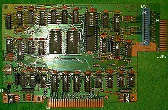
PE-box connector
Connections #2 to 60 on this side, connections #1 to 59 on back side
244: three 8-bit buffers, 74LS244 for the address bus and
control
lines.
245: A 8-bit transceiver, 74LS245 for the data bus.
125: A quad 74LS125 buffers, for 3-state output signals
(e.g.
RDBENA* , READY*, EXTINT*).
7805: Voltage regulator, TL780-05C, +5 volts. Nearby, is a
47uF
bypass cap.
7812: Voltage regulator, 78M12C, +2 volts. Nearby, is a 47uF
bypass cap.
-5: Negative voltage regulator, 79L05A, -5 volts
CRU logic
259: An 8-bit addressable latch, 74LS259 for CRU output
operations.
251: An 8-to-1 multiplexer, 74LS251 for CRU input operations
(unbuffered CRUIN line to the PE-box).
T: A transistor 2N3904 to control the LED.
LEDs: A yellow light-emitting diode reacts to CRU bit 0.
Address selection logic
Custom: Custom control IC: 1500280-1 DCM00MI8240.
27: Half a dual 3-input OR gates 74LS27.
30: An 8-imput AND gate 74LS30.
11: One gate out of a triple 3-input AND gates, 74LS11
(another
gate handles the reset signal, with a 47 uF cap. The third gate is
unused).
Wait-state logic
74: A dual flip-flop 74LS04
32: Two gates out of a quad OR gates 74LS32
27: One gate out of a triple 3-input OR gate 73LS27
04: Three inverters out of hex inverter chips 74LS04
Drive interface
DSK1: A 34-pin connector for the internal drive (odd pins
are
all grounded).
DSK2: A 34-pin card-edge for external drives (odd pins on
the
back side, all grounded).
74: Two dual flip-flops 74LS74.
123: Three one-shots out of two dual one-shot 74LS123. The
last
one generates the motor strobe pulse (47 uF cap).
00: Six gates out of two quad NAND gates 74LS00
04: Three inverters out of a 74LS04. All the above serve to
demultiplex the READ signal from the drive.
244: An 8-bit buffer 74LS244 for input lines from drive.
38: A triple-NAND gate, 74LS38. Output to the drive. On some
boards: two piggy-backed chips (???).
16: Hex-inverter 7416 (not LS). Output to the drive.
2901: A 12V buffer LM2901N. Drive selection feedback to the
74LS251 (???).
ROM
ROM: Two 4K ROMs, one for odd bytes, one for even bytes.
Labelled
DBT8240 (both), CD3233A & CD3234A. Controlled by the custom IC.
Controller
FD1771: Floppy disk controller. Western digital, FD1771B-01,
socketed.
Xtal: Crystal 8.0000 MHz.
04: Two 74LS04 inverters mounted as a flip-flop driven by
the
crystal.
00: Two NAND gates, out of a 74LS00. Mounted as inverters to
buffer the clock signal.
161: A counter74LS161 to divide the crystal frequency.
139: Half a dual 2-to-4 decoder (controls WE* and RE*
lines). Also
uses a 74LS32 OR gate.
Unused gates
04: Three inverters (from 3 distinct chips).
16: One inverter
11: A 3-input AND gate
27: A 3-input OR gate
244: One buffer gate.
139: Half a dual 2-to-4 decoder
For more details, see my page on the FDC
card.
Revision 1. 8/25/01. OK to release.
Back to the TI-99/4A Tech Pages