
Horizon Ramdisk
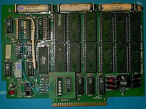
Shown here is a 1.5 Megabytes Horizon Ramdisk 3000, with RAMBO board
installed. All chips are socketed except on the RAMBO board.
Previous versions of this board may look differently. Also,
different
memory configurations are possible, and several modifications could be
made (Phoenix, RAMBO, 32K).
PE-box connector
Connections #2 to 60 on this side, connections #1 to 59 on back side
244: Two 8-bit buffers, 74LS244 for the address bus and
control
lines.
245: A 8-bit transceiver, 74LS245 for the data bus.
7805: Voltage regulator, UA7805, +5 volts. Three caps under
the heat sink.
Backup power
Bat: Three NiCad batteries 1.2V, 0.18 AH. They power
the
SRAMs and the 74HC154 (which is why these are HC instead of LS).
CRU logic
DIP: An 8-switches DIP switch to select a CRU address
between
>1000 and >1700.
138: Two 3-to-8 decoders, 74LS138 (one for the switch, one
to
select the proper '259).
259: Two 8-bit addressable latch, 74LS259 for CRU output (16
bits).
T: A transistor NTX2N2222A to control the red LED.
T2: Another 2N2222, not mentionned on the schematics. Used
to
control the green LED ??
LEDs: A red light-emitting diode reacts to CRU bit 0. A
green
LED (barely visible over green background) is connected to the CS2 pin
of the DSR RAM for test purposes.
Memory
SRAM: In this case, twelve HM628128LP-10 static RAM, 128
Kbyyes
each (total = 1.5 megs).
DSR: A SRM2264C static RAM, 8 Kbytes.
Selection logic
138: A 3-to-8 decoder, 74LS138 (under the RAMBO board).
156: Half a dual 2-to-4 decoder, 74LS156. (Was under the
RAMBO
board, now on it).
SW: Main switch that prevents the DSR from showing up at
>4000-5FFF.
Memory paging logic
138: A 3-to-8 decoder, 74LS138.
154: A CMOS 3-to-16 decoder, 74HC154.
U2b: Socket for another '154 to support 12 more SRAM chips,
piggy-backed on the existing ones.
Also used by the Phoenix modification.
Phoenix modification
Mainly for use with the "Geneve". Splits the Ramdisk in two:
a small boot drive controlled by 8 CRU bits, and a larger ramdrive
controlled
by 16 bits. When installed in a TI-99/4A such a modified board will
appear
as two Ramdisks having different CRU addresses.
The board shown above has not been modified, but carries the
necessary
sockets so that the modification can easily be made.
U25: Socket for a 74LS00 quad AND gates. Two gates selects
two
CRU addresses, the other two are mounted as a flip-flop to count the
number
of CRU bits written (8 vs 16), i.e. select the drive.
SW2 & SW3: Room for two additional switches to
toggle
between "TI-99/4A" and "Geneve" modes.
The Phoenix modification also implies re-wiring some of the 74LS138
and using two 74LS154.
RAMBO board
The RAMBO board lets you access part of the Ramdisk memory at CPU
memory
in the area >6000-7FFF.
RAMBO: A programmable logic array (PAL) that contains all
the
necessary logic gates.
156: The RAMBO board is plugged into the socket meant for a
74LS156. For this reason, a new 74LS156 is present on the board.
The blue wires are the various connections of the RAMBO chip. One
goes
under the board, to a bent-out pin of the 74LS138 that lies under here.
32K modification
This modification adds some memory so that the board duplicates as a
32K memory expansion. It involves the following:
Piggy-backing a 32K SRAM chip on top of the DSR chip. HM62256-LP12
or 43256-12L.
Piggy-backing a 74LS08 quad-AND gates on top of the 74LS138 that's
near the DIP-switch (just for power supply, no common pins).
Obviously, the board show here doe not carry this modification.
For details, see my Horizon Ramdisk page.
Revision 1. 8/26/01. OK to release.
Back to the TI-99/4A Tech Pages