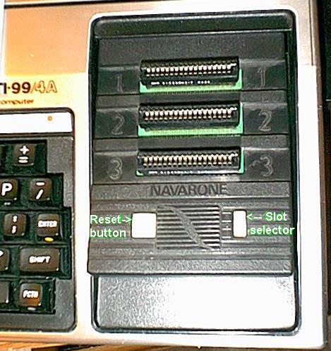
The little gadget known as the "Widget" is nothing more than
an extension plug that lets you have three cartridges plugged into the
cartridge port. A 2-position switch on the Widget lets you select which
cartridge is visible to the TI-99/4A. A push-button lets you reset the
TI-99/4A, since switching cartridges will not do it, as opposed to what
happened when you physically plug in a new cartridge.
NB I was told that the original spelling was "Widgit", but since everybody refers to it as Widget, that's how I'm going to call it.
The Widget was marketed by Navarone Industries. Its advantages are the following:
Hardware description
Modifying the Widget
_Material needed
_Preparing the Widget
_Preparing the chips
_Connecting the chips
to the
Widget
_Testing your work
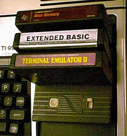
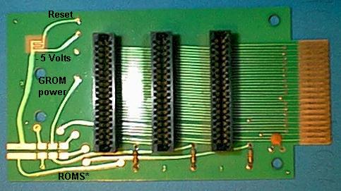
First, here are some pictures:
Widget plugged into the console, with no
cartridges
yet
Widget with three cartridges plugeed in
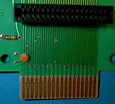
Under-the-hood picture, top side
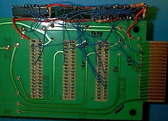
Ditto, bottom side of the PCB
Schematics:
o-------> Connector #1, pin |
Hardware-wise, the Widget is very simple. Three card-edge connectors, like the one in the console, are wired in parallelel on a small printed-circuit board, that can be plugged in like a cartridge.
All lines go directly from the cartridge port to the three connectors, except for two lines:
The reset button simply connects the -5V power supply to the Reset*
line in the console port. No debouncing circuitery is provided.
As you know, the TI-99/4A makes provision for several GROM bases: one
at
>9800, one at >9804, one at >9808, etc. The console GROMs and
the GROMs inside any cartridge plugged into the cartridge port, answer
to each and every base. But theoretically, we could have upto 16
cartridges
plugged in, if we could design a circuitery that would install each
cartridge
at a different base. The Widget is a good base to implement such a
modification,
at the cost of only 4 TTL chips (total cost, about $6).
After this modification, all three cartridges in the Widget are visible to the TI-99/4A. The first one appears on the main menu under TI-Basic. It is followed by an item saying "Review Module Library". Selecting this option will make the second cartridge appear in the menu, then the third, then the first one again.
This modification is based on an original idea by Randy McVicar, who suggested it in the on-line user group for the TI-99/4A, http://groups.yahoo.com/group/ti99-4a It got me thinking and I came up with the following solution:
In the schematics below I'm using ports >9800 for slot #1, >9808 for #2 and >9810 for #3. You can choose other ports by picking different Yx* lines from the 74LS138, and/or by swapping around lines A10 through A13.
If you don't like my "ascii art", here is a jpeg version, courtesy Andrew Deschenes.
+5V----++, |
The heart of the modification is a 74LS138 decoder. It decodes the four address lines, A10 to A13 into 8 distinct bases (out of a total of 16). You can choose which bases will be available by deciding which address line should go to the G2A* enabling input.
G2A*   A10     A11     A12     A13
S2     A11     A10     A10     A10  etc (12 possible permutations)
S1     A12     A12     A11     A11
S0     A13     A13     A13     A12
Y0    >9800   >9800   >9800   >9800
Y1    >9804   >9804   >9804   >9808
Y2    >9808   >9808   >9810   >9810
Y3    >980C   >980C   >9814   >9818
Y4    >9810   >9820   >9820   >9820
Y5    >9814   >9824   >9824   >9828
Y6    >9818   >9828   >9830   >9830
Y7    >981C   >982C   >9834   >9838
Pick a combination that contains three bases that you would like to use. Normally, you should always have >9800 for your first slot, since some poorly written cartridges will only work from this base. Be aware that the routine that builds up the cartridge menu only adds the "Review module library" item if it detects a difference between adresses >6000-601F at base >9800 and at base >9804. So it may be a good idea to pick >9804 for the second slot. This way, as long as there is one cartridge in either of these slots, all three will be scanned. For the last slot I chose >9810, but it's really up to you. If you have a GRAM card, you may want to select bases that do not interfer with it...
The decoder does not control the -5V power line, because I could not figure out how to control negative voltage with TTL gates. Instead, it controls the GS* line, that signals GROM operations (Grom Select, active low). The -5V power supply lines are connected together, bypassing the switch.
This raises a delicate problem with the GR line (Grom Ready). The GROMs use this line to put the TMS9900 microprocessor on hold, until they are done storing/retrieving data. You might expect that, when GROMs are not selected, this line would be inactive. Well, no: it's always inhibitory, except when the GROMs are ready! To avoid locking up the computer, there is a small circuitery in the console that intercepts this lines and only enables it during GROM operations. But now, we have three cartridges connected to this line, and only one will see GROM operations: the other two will send wait signals on the line, which will lock up the computer.
This is the reason for the second chip, a 74LS32 quad OR gates. For each slot, the GR signal is combined with the GS* line provided by the 74LS138 decoder. Which means that the output can only be low if the cartridge is actually being selected, otherwise the GROM complaints are just ignored. Note the 4.7 kOhms pull-up resistors on the GR lines: they insure that the line will remain high even if no cartridge is plugged in.
One difficulty is that the three outputs should be connected
together.
However, we don't want the two "high" lines to fight the "low"
one. The ideal solution would be open-collector OR gates, but for some
reason there is no such TTL. The next best thing was to have a 3-state
buffer controlled by the OR gate: a low signal will enable the buffer,
which will issue a low output, since its input is tied to ground. A
high
signal from the OR gate leaves the buffer in high-impedance, i.e.
isolated.
The outputs of the three buffers can thus be tied together and fed to
the
console GR line: the one that is active will bring the line low, the
other
two will not affect the line.
All this is nice and fine, but it only works for GROMs. Yet, many cartridges also have ROM onboard, which maps in the area >6000-7FFF. Now, suppose we have three such cartridges plugged into the Widget: how are we going to decide which one should have its ROM appearing at >6000-7FFF?
This is the purpose of the 74LS374 latch: it remembers which GROM was accessed last, and enables the corresponding ROM when a ROM operation occurs. The chip can latch upto 8 lines, but for our purpose it is sufficient to latch the three outputs of the 74LS138 that are used to select cartridges.
The 74LS374 latches data when its Clk pin goes from low to high. This pin is fed a combination of GS* (from the console), WE* (write enable, from the console) and A14 (high for GROM address operations). GS* and WE* are combined with an OR gate, whose output enables the remaining 3-state buffer in the 74LS125. Its input is connected to A14 and its output to a 4.7K pull-down resistor. As a result, the 74LS374 see a low-to-high transition on its Clk pin when GS* and WE* are low, and A14 is high will . Which occurs each time you write a new GROM address to any base.
Finally, the OE* (output enable) pin, is controlled by the ROMS* line. The three selected outputs of the 74LS374 go to the ROMS* lines in the three cartridge connectors. Normally, we would add pull-up resistors on these lines, but the Widget already contains them, which makes our life even easier. All we need is one resistor on the OE* pin so that it remains high when the switch is not in position #1.
Finally, what about pure ROM cartriges? Here, there is no software
solution,
as the TI-99/4A operating system does not contain any provision for
multiple
ROM cartridges. We will thus need to use the Widget switch with such
cartridges.
We'll just modify the switch's wiring so that position #2 and #3 work
as
before, whereas position #1 selects our latch circuit. The only problem
is that the routine that builds the main menu does not handle ROM
cartridges
properly when the switch is in position 1 (because it last writes to
>9804
before scanning the ROMs, but writes to >9800 before building the
menu
screen). So you cannot have a pure ROM cartridge in position #1, sorry.
But you can have pure ROM cartridges in positions #2 and #3, if you
select
them with the switch.
Open the Widget. There are four Philips screws to be removed, then you
can just open the cover and remove the PCB (printed circuit board).
Store
switches and screws in a safe place since you will need them later.
Flip over the PCB and identify the connections we are going to use.
It may be a good idea to identify them with a marker...
To console
   ROMS*               A11 A13
    | WE*            A10|A12|     Ground
    | |               | | | |       |
  X X X X X X X X X X X X X X X X X X   #1
  X X X X X X X X X X X X X X X X X X
  |   |       | | |
Gnd  GR     A14 | +5V
   ROMS*       GS*
    |
  X X X X X X X X X X X X X X X X X X   #2
  X X X X X X X X X X X X X X X X X X
      |         |
     GR       GS*
   ROMS*
    |
  X X X X X X X X X X X X X X X X X X   #3
  X X X X X X X X X X X X X X X X X X
      |         |
     GR       GS*
                 To user
Because space is limited whithin the Widget, I chose not to implant the chips on a PCB, but rather to wire them directly. It does not look as nice, but it's way easier.
Let's first do the internal connections for each chip. In the diagrams below, the chips are viewed from above. The notch (or tiny dot) that marks pin #1, is at the top of the page, represented here with --++--
74LS32 (14 pins)
          ,--------------,
          |  +---++---+  |     R = 4.7K resistors
          R [|1A   Vcc|]-+-,
          '-[|1B    4A|] R |
            [|1Y    4B|]-' |
            [|2A    4Y|]   R
            [|2B    3A|]   |
            [|2Y    3B|]---'
            [|Gnd   3Y|]
             +--------+
74LS125 (14 pins)

             +---++---+    R = 4.7K resistor
            [|1G*  Vcc|]
            [|1A   4G*|]
          ,-[|1Y    4A|]-,
          R [|2G*   4Y|]-|-,
          +-[|2A   3G*|] | |
        ,-|-[|2Y    3A|]-+ |
        | +-[|Gnd   3Y|]-|-'
        | |  +--------+  | |
        | '--------------' |
        '------------------'
74LS138 (16 pins)
          ,--------------,
          |  +---++---+  |
          | [|S0   Vcc|]-'
          | [|S1   Y0*|]
          | [|S2   Y1*|]
          | [|G2A* Y2*|]
          | [|G2B* Y3*|]
          '-[|G1   Y4*|]
            [|Y7*  Y5*|]
            [|Gnd  Y6*|]
             +--------+
74LS374 (20 pins)
          ,----R---------,
          |  +---++---+  |
          '-[|OE*  Vcc|]-'
            [|Q1    Q8|]
            [|D1    D8|]
            [|D2    D7|]
            [|Q2    Q7|]
            [|Q3    Q6|]
            [|D3    D6|]
            [|D4    D5|]
            [|Q4    Q5|]
            [|Gnd  Clk|]
             +--------+
Now arrange the 4 chips in a file, making sure they would fit inside the Widget box, along the right side of the PCB. My favorite arrangement was: 32-125-138-374, but feel free to choose another solution.
Wire the chips together like this (viewed from the top):
             +---++---+
    ,-------[|1A   Vcc|]-,
    |       [|1B    4A|]-|-----,
    |   ,---[|1Y    4B|] |     |
  ,-|---|---[|2A    4Y|]-|-,   |
  | |   |   [|2B    3A|]-|-|---|-,
  | | ,-|---[|2Y    3B|] | |   | |
  | | | | ,-[|Gnd   3Y|]-|-|-, | |
  | | | | |  +--------+  | | | | |
  | | | | |              | | | | |
  | | | | |  +---++---+  | | | | |
  | | '-|-|-[|1G*  Vcc|]-+ | | | |
  | |   | | [|1A   4G*|]-|-' | | |
  | | ,-|-|-[|1Y    4A|] |   | | |
  | | | '-|-[|2G*   4Y|] |   | | |
  | | |   | [|2A   3G*|]-|---' | |
  | | |   | [|2Y    3A|] |     | |
  | | |   +-[|Gnd   3Y|] |     | |
  | | |   |  +--------+  |     | |
  | '-|---|--------------|-,   | |
  |   |   |  +---++---+  | |   | |
  |   |   | [|S0   Vcc|]-+ |   | |
  |   |   | [|S1   Y0*|]-|-|---+ |
  |   |   | [|S2   Y1*|]-|-|---|-+
  |   |   | [|G2A* Y2*|] | |   | |
  '---|---|-[|G2B* Y3*|] | |   | |
      |   | [|G1   Y4*|]-|-+   | |
      |   | [|Y7*  Y5*|] | |   | |
      |   +-[|Gnd  Y6*|] | |   | |
      |   |  +--------+  | |   | |
      |   |              | |   | |
      |   |  +---++---+  | |   | |
      |   | [|OE*  Vcc|]-' |   | |
      |   | [|Q1    Q8|]   |   | |
      |   | [|D1    D8|]---'   | |
      |   | [|D2    D7|]-------|-'
      |   | [|Q2    Q7|]       |
      |   | [|Q3    Q6|]       |
      |   | [|D3    D6|]-------'
      |   | [|D4    D5|]
      |   | [|Q4    Q5|]
      |   '-[|Gnd  Clk|]-,
      |      +--------+  |
      '------------------'
It's easier to work from the bottom side of the Widget, since the
connector
pins are more accessible this way. Therefore, in the following diagram,
the chips are viewed from under. When a connection bears no #, it means
that you can use whichever of the three slot connectors is the most
convenient.
Otherwise, use the one I specified: #1 being the closest to the
console,
#3 the closest to you. The connections labelled "console" should
be made on the console side of your cuts; convenient places are the
"via"
that bring the lines from the other side of the PCB.
Console side
                       A11 A13
  ROMS*              A10|A12|     Ground
    |                 | | | |       |
  X X X X X X X X X X X X X X X X X X   Slot viewed
  X X X X X X X X X X X X X X X X X X   from under
  |   |         | |
  |  GR         | +5V
Ground        GS*

           Your side
        Chips viewed from UNDER
              +--------+
             [|Vcc   1A|]
             [|4A    1B|]---------#3/GR
 #1/GR-------[|4B    1Y|]
             [|4Y    2A|]
             [|3A    2B|]---------WE*
 #2/GR-------[|3B    2Y|]
             [|3Y   Gnd|]
              +--------+

              +--------+
    +5V------[|Vcc  1G*|]
             [|4G*   1A|]---------A14
             [|4A    1Y|]
             [|4Y   2G*|]
             [|3G*   2A|]
             [|3A    2Y|]
Console/GR---[|3Y   Gnd|]---------Ground
              +--------+
              +--------+
             [|Vcc   S0|]---------A13
 #1/GS*------[|Y0*   S1|]---------A12
 #2/GS*------[|Y1*   S2|]---------A11
             [|Y2* G2A*|]---------A10
             [|Y3* G2B*|]-----Console/GS*
 #3/GS*------[|Y4*   G1|]
             [|Y5*  Y7*|]
             [|Y6*  Gnd|]
              +--------+
              +--------+
             [|Vcc  OE*|]-----Switch cut-off position #1
 #3/ROMS*----[|Q8    Q1|]
             [|D8    D1|]
             [|D7    D2|]
 #2/ROMS*----[|Q7    Q2|]
 #1/ROMS*----[|Q6    Q3|]
             [|D6    D3|]
             [|D5    D4|]
             [|Q5    Q4|]
             [|Clk  Gnd|]
              +--------+
And that's it! Fasten the wires in place with some electrical tape,
then
install the PCB and the chips back into the Widget box. The chips
should
fit easily along side the PCB. You may want to tape them in place.
Here is a couple of pictures of the modified Widget: viewed from the top, and from under.
Finally, put the switches back in place (beware that the selector
switch
is not symetrical: it has small bumps on one side), close the lid and
gently
fasten the screws.
At this point, you are probably dying to test your new and improved
Widget.
Don't. Until now, any mistake you may have made did not have
consequences,
because the Widget only contains inert components. However, you are now
about to plug it into your TI-99/4A and a miss-wiring may actually
damage
the console!
So make up your mind that you will not test the Widget before at least one hour. Spend this hour checking all the connections you made. If you own a continuity tester, now is the time to put it to work. Then check again, and again, until you are 100% confident that you did not make any mistake (personally, I made several...).
Now check for shortcuts between adjacent pins: it's easy to accidentally make a solder bridge... Finally, check for a shortcut between ground and power supply, the most dangerous type.
Now you can begin your tests:
First, plug in the emtpy Widget, with the switch in position 1. Turn on the console, with no PE-Box: it should power on normally and you should only see TI-Basic on the main menu. If the TI-99/4A does not boot, there is most probably a problem with your wiring of the 74LS125.
Then power off the console, and install three GROM cartridges into the Widget. Power the console again. You should the cartridge in slot #1 appear after TI-Basic on the main menu. The last item in the menu should be: "Review module library". Select it: the menu should change to display the cartrige in slot #2. By repeatedly selecting "Review module library" you can circle between the three cartridges. If the console does not boot, check for a mismatch between the GR lines going to the 74LS32 and the GS* lines going to the 73LS138. If you only see the cartridge corresponding to the switch position, make sure you did not forget to shorcut the -5V part of the main switch.
You can test ROM switching with cartridges like Extended Basic, or Mini-memory. With XB make sure CALL INIT works no matter in which Widget slot the cartridge is inserted. With Minimem, enter EasyBug, type M6000 and see if it contains >AA. If this does not work, check the wiring of the 74LS374. In particular, make sure each output goes to the same slot than the corresponding output in the 74LS138.
To ensure that you selected the inteded bases, use the Extended Basic cartridge. Plug it into a slot and type: CALL LOAD(-31878,A,B), then PRINT A,B. A should be equal to 152 (>98) and B to the base corresponding to that slot (0, 4 and 16 in my example). If you get unexpected values, check the connections of A10 through A13 to the 74LS138.
If everything tests correctly, congratulations: you made it. Now
enjoy
your "Super-Widget" !