This page explains how to install an extra CRU interface inside the console: either up to 64 output bits, or up to 32 output and 32 input bits.
These extra CRU bits can be used to control the following console modifications:
Bill of materials
Principle
Doing it
Our CRU interface answers at address >0400, in between the addresses reserved by the TMS9901 (although it only uses 64 bits, the TMS9901 reserves 512 due to incomplete decoding) and the addresses used by peripheral cards (>1000 and up).
Address decoding is performed by a 74LS138 decoder. Note that our decoding also is incomplete and reserves 8 times more bits than it can actually use. The decoder can be wired in two ways, depending on whether you want 64 output bits, or 32 input and 32 output bits. For the former, the CRUCLK* enables the whole chip via its G2B* pin, for the latter CRUCLK* is applied to one of the decoded inputs.
Here is the wiring for 64 output bits: each of the decoder's eight outputs can control a 74LS259, each of which can output eight bits. The OR gate combining A3 and A4 already exists in the console: it's part of the decoding circuit for the TMS9901 and the scratch-pad RAM.
74LS138 74LS259 |
And here is the alternate wiring, in case you prefer an input/output solution. As you can see, it only exchanges CRUCLK* and A9. Note that it is not neccessay for the 74LS251 to read back all the bits issued by the 74LS259: you could use some (or all) bits to sense other hardware conditions. Your imagination is the limit, here...
74LS138 |
The easiest way to install extra chips inside the console is to piggy-back them on top of existing 16-pin chips, connecting only their power supply pins (#8 and #16). All input signals are available in the console, most of them near the side port, which is thus a good location to implant your chips. If you're going to use many 74LS259 (or 74LS251) you may want to stack two of them on top of a console chip.
Below is a description of the most basic implementation, with only one 74LS259 that provides 8 output bits. In most cases, this will be more than enough. (Besides, it's the only one I've tested so far...).
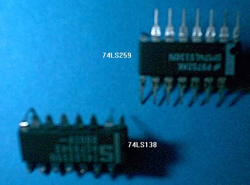
Lets first prepare the two new chips: a 74LS138 decoder and a 74LS259 addressable latch. These are very common TTL chaps that can be obtained for less than $1 in any electronics store.
With forceps or small pliers, delicately grab each pin and bend it out until it's horizontal. Do not bend pin #8 (bottom left), not #16 (upper right): these will be soldered to the corresponding pins on the supporting chip. On the 74LS259 also leave pin #2 unbent: we're going to piggy-back it on a chip that happens to have the proper signal on pin #2.
Using a wire cutter, trim the bent out pins at the point where the pin becomes narrower (i.e. from |==-- to |== ). This is necessary because chips are so close to one another in the console that bent out pins would touch each other. Here is a picture in which the 74LS138 is ready, whereas the 74LS259 still needs trimming.
Refer to my console surgery page for instructions on how to take apart the TI-99/4A console.
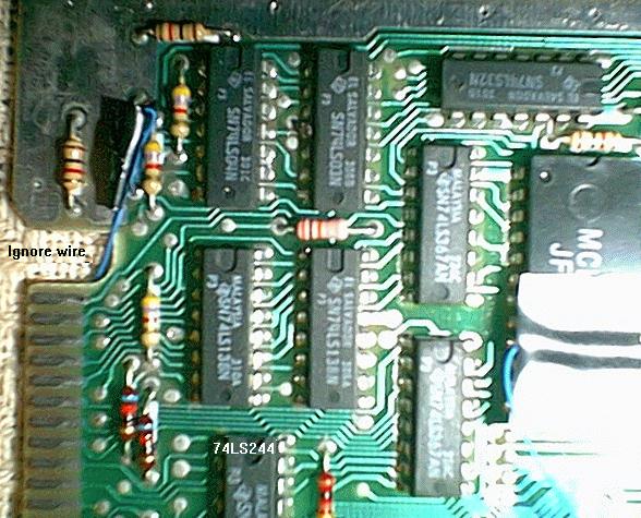
Locate the relevant chips, near the side port. Here is a picture to help you.
Attach wires to the relevant chips; make them a bit longer than necessary so you have some margin to work with. I'm using gauge 30 (i.e. wire-wrap type) wire. I strip the end on about 1 cm, to form a tiny hook with it and pass it around the pin I want. Then I use forceps to pull it further out and twist it on itself. A tiny drop of solder is enough to complete the joint between wire and pin.
A faster (but less secure) way is to deposit a drop of solder on/alongside a pin, then dip the end of the wire in the molten solder and wait for it to harden and secure the connection. In any case, make really sure that the solder will not make contact with neighbouring pins or tracks, nor with any (future) piggy-backed chip.
Refer to the following diagram for necessary connections: the numbers indicate pin numbers. All chips are in the corner where the side port is, except for the CruOut signal that can be found on a 74LS32 chip, on the other side of the big TMS9900 microprocessor (see diagram further down).
    __
 __|  |    ,-- Piggy-back new 74LS04 on this '04 (optional).
|     |____V____________________________________________
|       74LS04      74LS03         A3uA4---,
|       +-,_,-+     +-,_,-+      +---------'----+
|       |     |     |     |      |         3   ,|
|       |     |     |     |      | 74LS32      '|
|Reset*-|3    |     |     |      +--------------+
|       |     |     |     |     +-,_,-+
|       |     |     |     |     |     |
|       |     |     |     |A5---|2    |
|       |     |     |     |     |   14|---A10
|       +-----+     +-----+     |     |
|       +-,_,-+     +-,_,-+     |   12|---A11
|       |     |     |     |     |     |
\___    |     |     |     |     |   10|---A12
 ___|   |     |     |     |     | 367 |
|===    |     |     |     |     +-----+
|===    |     |     |     |     +-,_,-+
|===    | 74  |     | 74  |     |     |
|===    | LS  |     | LS  |     |2=A13|
|===    | 138 |     | 138 |<-,  |   14|---A14
|===    +-----+     +-----+  |  |     |
|===        +-,_,-+          |  |   12|---A9
|===        |     | Piggy-back  |     |<--- Piggy-back new 74LS259
|===        |     | new '138    |     |     on this 74LS367
|===        |     | on this     |     |
|===        |     | 74LS138     +-----+         +-,_,-+
|===        |     |             74LS367         |     | Far
|===        |   15|---CruClk*                   |     | away ===>
|===        |     |              This chip ---->|     |
|===        |     |              is on the      |     |
|===        |     |              other side     |     |
|===        |     |              of the big     |    9|---CruOut
|===        +-----+              TMS9900        |     |
|===        74LS244                             +-----+
|===                                             74LS32
Install the 74LS138 on top of another 74LS138 in the console (e.g. U505). Solder pin #8 and #16 to the same pins on the console chip. Make sure the other pins do not make contact with the underlying chip.
Install the 74LS259 on top of the second 74LS367 (U503). Solder pin #2, #8 and #16 to the underlying chip. If you are installing another 74LS259 elsewhere, bend out its pin #2 as the underlying chip won't have A13 on that pin.
Now connect the wires you have previously installed to the cut-out pins of the piggy-backed chips. Be carefull with solder, that it does not flow to the underlying chip. Refer to this diagram for connections.
    __
 __|  |
|     |__________________________________________
|       74LS04
|       +-,_,-+     +-,_,-+      +--------------+
|       |     |     |     |      |             ,|
|       |     |     |     |      |             '|
|       |     |     |     |      +--------------+
|       |     |     |     |     +-,_,-+
|       |     |     |     |     |     |
|       |     |     |     |     |     |
|       |     |     |     |     |     |
|       +-----+     +-----+     |     |
|       +-,_,-+     +-,_,-+     |     |
|       |     |A11--|1  16|]    |     |
\___    |     |A10--|2  15|-,   |     |
 ___|   |     |A9---|3  14| |   |     |
|===    |     |A3u4-|4  13| |   +-----+
|===    |  CruClk*--|5  12|     +-,_,-+         |
|===    |     |A5---|6  11|A14--|1  16|]        |
|===    |     |     |7  10|    [|2  15|--Reset* |
|===    |     |    [|8   9|A12--|3  14|---------'
|===    +-----+     +-----+  B0-|4  13|--CruOut
|===        +-,_,-+ 74LS138  B1-|5  12|--Bit7
|===        |     | on top   B2-|6  11|--Bit6
|===        |     | another  B3-|7  10|--Bit5
|===        |     | 74LS138    [|8   9|--Bit4
|===        |     |             +-----+
|===        |     |         74LS259 on top of
|===        |     |            a 74LS367
|===        |     |
|===        |     |
|===        |     |    [| = solder to underlying chip
|===        |     |    B0-Bit7 = CRU bits for you to use
|===        +-----+
|===
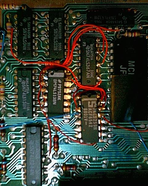
Here's a picture of this stage. The blue wire is connected to Bit0 for test purposes. The piggy-backed chips still need to be covered with insulating tape, to make sure they won't contact the metal shell that's around the motherboard.
Now all you need to do is to connect the outputs of the 74LS259 to the devices you want to control. In order, these are pins #4 through #7, then #9 through #12.
Remember that all outputs will be low at power-up time. If you need a bit to be high by default, you should connect the corresponding output to an inverter. There are several free inverters on the 74LS04 that's alongside the "far away" 74LS32: look for unconnected pins ( #5-|>o-#6, #11-|>o-#10, #13-|>o-#12). Be aware that unused inputs may be grounded (only pin #13 was in my console). In this case, you should either cut and bend out the pin, or cut the trace that connects it to the ground.
                  +-,_,-+        74LS00       74LS00
                  |     |        +-,_,-+      +-,_,-+
                  |     |        |     |      |     |
                  |     |        |     |      |     |
                  |     |        |     |      |     |
                  |     |        |     |      |     |
                  |     |        |     |      |     |
                  |     |        |     |      |     |
                  +-----+        |     |      |     |
                  74LS00         +-----+      +-----+
                                 +-,_,-+      +-,_,-+
                                 |     |      |     |
    ,---CruIn                    |     |      |   13|-- In (grounded)
    |         CruOut---------,   |     |      |   12|]- Out
    |                        |   |     |      |   11|-- In
+-'-'- . . . --'-'-'-'-'-+   |   |     | In --|5  10|]- Out
| 3 3          5 4 3 2 1 |   '--------9| Out-[|6    |
| 2 1                    |       |     |      |     |
|                       |        +-----+      +-----+
|      . . .   TMS9900  |         74LS32       74LS04
|                        |       +-,_,-+
|                        |       |     |
+-,-,- . . . --,-,-,-,-,-+       74LS04
Alternatively, you can piggy-back an additional inverter of your own on
top of a 14-pin chip (such as the 74LS04 that's in the corner). Bend
out
and trim all its pins, except for #7 and #14 that need to be soldered
to
those of the underlying chip. This will give you 6 inverters,
conveniently
closed to the newly intalled 74LS259. This is the solution I chose for
my console. The pinout of a 74LS04 is the following:
      +-,_,-+
  In--|,    |]
 Out--|'   ,|--In
  In--|,   '|--Out
 Out--|'   ,|--In
  In--|,   '|--Out
 Out--|'   ,|--In
     [|    '|--Out
      +-----+
If you need more than 8 bits, you can connect additional 74LS259s to the remaining outputs of the 74LS138: in order, use pin #15 through pin #9, then pin #7.
                  74LS138
                  +-,_,-+
                  |     |
                  |   15|---> Bits 0 to 7
                  |   14|---> Bits 8 to 15
                  |   13|---> Bits 16 to 23
                  |   12|---> Bits 24 to 31
                  |   11|---> Bits 32 to 39
Bits 56 to 63 <---|7  10|---> Bits 40 to 47
                  |    9|---> Bits 48 to 55
                  +-----+
Piggy-back the additional 74LS259 on top of 16-pin chips. If necessary, stack them two-deep. The wiring of every 74LS259 is identical, except from pin #14, which should be connected to one of the 8 outputs of the 74LS138 shown above.
If you want CRU input, you will need one (or more) 74LS251. Bend out and trim all its pins, except for pin #8 and #16. Then install it on top of a 16-pin chip, and solder pin #8 and #16 to those of the underlying chip. Connect the other pins as per the diagram below. This will give you 8 input bits per 74LS251.
Remember that you will also need to swap A9 and CruClk* when piggy-backing the 74LS138. This way, its pins #15 through #12 control four 74LS259 for CRU output, and pins #11 through #9 and #7 control four 74LS251 for CRU input.
               74LS138                      74LS251#1
               +-,_,-+                      +-,_,-+
          A11--|1    |]               Bit3--|1    |]
          A10--|2  15|--->74LS259#1   Bit2--|2  15|--Bit4
      CruClk*--|3  14|--->74LS259#2   Bit1--|3  14|--Bit5
        A3uA4--|4  13|--->74LS259#3   Bit0--|4  13|--Bit6
           A9--|5  12|--->74LS259#4      ,--|5  12|--Bit7
           A5--|6  11|----------------,  |  |6  11|--A14
  74LS251#4<---|7  10|--->74LS251#2   '--|--|7  10|--A13
              [|    9|--->74LS251#3      | [|    9|--A12
               +-----+                   |  +-----+
                                         '---------->TMS9900 pin #31
                                                     (see CruIn above)
N.B. I didn't test this modification...
Make sure that none of the piggy-backed chips is making contact with the metal shell that comes on top of the motherboard. If necessary, insulate them with electrical tape.
Then close the console as instructed in my console surgery page.
You can test any CRU output that you have connected by checking if the corresponding feature can be turned on/off via the CRU (duh !).
Alternatively, you could solder a long wire to a free output and feed it through a venting slot in the console. Connect it to a voltmeter and see if the voltage changes when you toggle the corresponding CRU bit.
The easiest way to toggle CRU bits is to use a debugger, such as EasyBug (in the Mini-memory cartridge), MG's Explorer, or my Module Explorer (downloadable here). Remember that the address will be >0400 through >0410 for the first 8 bits, as CRU adresses increment by two (i.e. only even addresses are used).