The TI-99/4A console and peripheral card ROMs contain a number of obnoxious bugs and short-sighted design decisions. How many times did you think "If only TI programmers hadn't..."? Unfortunately we have to live with these problems, since they are engraved in stone, I mean in ROM.
Or do we? Why not replace the buggy ROM with a brand new EEPROM that would let us introduce as many patches and improvements as we want? This page is inteded to explain how to perform such a modification. As you will see, it's fairly easy to do and does not require any prior knowledge in electronics.
Introduction
_Taxonomy of ROMs
_EEPROMs employed
_Tools required
Before we start, just a few definitions.
For the modifications described in this page, we are going to use the following chips:
Atmel AT28C64. This is an 8 kilobytes EEPROM, suitable for
in-circuit
programming. It latches only one byte at a time, and does not require
any
unlocking sequence. Turned out to be sold out when I placed my order,
so
I went instead for the
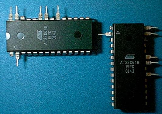
Atmel AT28C64B which is a fancier version of the above. It can
latch
upto 64 bytes at a time and has an optional write-protection sequence.
It's also a bit more expensive: I bought mine from Digikey for about
~$5.00
each (vs $3.38 for the non-B).
Xicor X28HC64. This is also an 8K EEPROM, suitable for in-circuit programming as it can latch more than one byte and offers an optional code protection by an locking/unlocking sequence. It's superior to the Atmel "B" chip in that it can be programmed one million times, versus 10,000 to 100,000 for the Atmel chips. Of course, it's also more expensive: Digikey sells them $9.63 a pop.
All three chips share the same pinouts, which are very similar to the 4K ROMs used in the TI-99/4A. Similar but not identical, since the EEPROMs have more pins: being 8K they need one more address pin (there are no 4K EEPROMs, the size goes by 4-fold increments), also they need a write-enable pin. However, the schematics below clearly indicates that, if both chip were alligned at the bottom, most of their pins would match, except for a few:
                                 EEPROM 28C64
                                +----+--+----+
       ROM 4732              nc |1 o       28| Vcc
     +----+--+----+         A12 |2         27| WE*
  A7 |1 o       24| Vcc      A7 |3         26| nc
  A6 |2         23| A8       A6 |4         25| A8
  A5 |3         22| A9       A5 |5         24| A9
  A4 |4         21| CS2*     A4 |6         23| A11
  A3 |5         20| CS1*     A3 |7         22| OE*
  A2 |6         19| A10      A2 |8         21| A10
  A1 |7         18| A11      A1 |9         20| CS*
  A0 |8         17| D8       A0 |10        19| D8
  D1 |9         16| D7       D1 |11        18| D7
  D2 |10        15| D6       D2 |12        17| D6
  D3 |11        14| D5       D3 |13        16| D5
 Gnd |12        13| D4      Gnd |14        15| D4
     +------------+             +------------+
One last word, on how to orient the chips. If you look carefully,
you
will notice that each chip carries a little notch on one of its ends:
this
indicates the top of the chip, where pin #1 is to be found. Sometimes
there
is no notch, but pin #1 will be indicated by small dot, either painted
on the chip or carved into it. By convention, numbering goes down along
the left side, then up along the right side.
Here is a picture of some of my tools. Don't panic, you won't need that many: I'm just showing off. What you will need is:
The DSRs of the RS232 card have an annoying bug that prevents us from using the built-in timers in the two TMS9902 chips. Also, delay loops for serial transmissions are taken from a value table in the card ROM. If you modify your console so that it runs at 4 MHz instead of 3 MHz, the RS232 ports become useless because the transmission speed is all wrong. Finally, there is enough room left in the DSR space so that we could add a few cool routines in there... This should be enough reasons for us to want to replace the card ROMs with EEPROMs.
For this modification, we are going to use a Xicor X28HC64, 8Kbytes EEPROM. An AT28C64 chip wouldn't do the job because it must be written one byte at a time, which we cannot do in the PE-box.
No big deal.
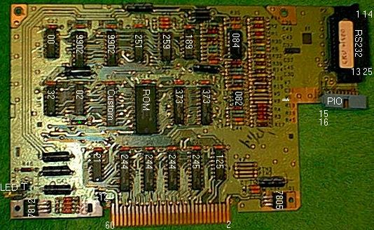
Refer to this commented picture to
identify
components on the card. You will identify the ROM easily, as it is the
only wide chip on board (0,6 inches, as opposed to the usual 0.3).
Here you have two options: you can remove the ROM chip completely, or you can install the new chip on top of it (piggy-backed, in EE lingo).
To remove the chip, you must desolder each pin and make sure its completely free of solder before you can pull the chip out. This is not as easy as it sounds, even with a desoldering pump! On the other hand, if you are willing to sacrifice this ROM chip, it will make things way easier. Just cut every pin, discard the chip, then desolder the pin stumps one at a time, pulling them out with forceps (as they will be HOT !).
Then cut a small length of gauge 26 wire (about an inch) strip the coating from one end and insert it on the hole where pin #24 used to be (the topmost on the right). Solder it in place, making sure to put solder on the side of the board where the connection trace is.
Install another such piece of gauge 30 wire in the hole where pin
#18
used to be.
If you chose to piggy-back chips, you will need to disable the ROM so that it won't answer together with the EEPROM. This can be done by rewiring pin #21 (CS2*), which is currently connected to ground. We'll just connect it to +5V and it will disable the ROM.
This is what the chip would look like, viewed from the right side.
                          ,-----+--------To EEPROM pin #28
Bottom   .================|=====|=, Top (pin 24)
(pin 12)  # # # # # # # # " # # #
                    '----To EEPROM pin #23
Here is a picture for you: the red wire (gauge 26) is for power supply, the blue wires (gauge 30) for signal lines. Here is another picture, after insulation with electrical tape.
Before you install the Xicor EEPROM, some preparation is needed:
The EEPROM should now look like this, viewed from the top:
             +---+--+---+
             | nc    Vcc|==-   To ROM pin #24
To switch -==| A12   WE*|==-   To 74LS02, pin #9
or 74LS259  [| A7    nc |         or switch
   pin #12  [| A6    A8 |]
            [| A5    A9 |]
            [| A4    A11|==-   To ROM pin #18
            [| A3    OE*|]
            [| A2    A10|]
            [| A1    CS*|==-  To custom chip pin #13
            [| A0    D8 |]
            [| D1    D7 |]     Legend:
            [| D2    D6 |]     |==- Stretched-out
            [| D3    D5 |]     |    Cut
            [| Gnd   D4 |]     |]   Normal
             +----------+
Here is a picture (out of focus, sorry).
If you removed the ROM, your job is to fit the narrow part of the EEPROM pins into the holes in the PCB. You may find that the two rows of pins are too far appart. This is normal and can be fixed easily: hold the side of the chip against the edge of a table, with all the pins (but the stretched ones) pressing against the table. Tilt the chip gently, so as to push the tip of the pins inwards, just a bit. Repeat on the other side.
Once the chip is in, solder each pin in place. First put the iron to
the pin and board for a second, to warm them up. Then touch the solder
wire to the tip of the iron and apply a drop of solder to the pin.The
solder
should spead evenly on both the pin and the copper pad on the board.
Repeat
on the other side of the board, in case the pin would have a connection
there also.
If you chose the piggy-back solution, install the EEPROM on top of the ROM, aligning them at the bottom. Here also you may have to narrow the pin rows a little, so the EEPROM clamps the ROM snuggly.
Now solder the EEPROM pins to the ROM pins. Put the iron to the pins
for a second, then touch the iron with the solder roll. Make sure the
drop
of solder speads on both pins, so it makes good contact. Tip: stand the
board on its edge, so that the pins you are laying solder on are
horizontal.
The wire that we have attached to ROM pin #24 (or the hole it was in) should go the steched-out pin #28 on the EEPROM. Solder it cleanly, then trim it quite short. This pin is the power supply and it's very important that it does not touch the metal case, at this would cause a nasty short-cut. I would advise you to cover the connection with a bit of insulating tape...
The wire that you attached to ROM pin #18 (A11) should be soldered to stretched out pin #23 on the EEPROM (A11, duh!).
Stretched-out pin #20 is the chip-select pin. We cannot connect it
the
the CS1* pin of the ROM, because this signal is only active for read
operations,
which is why we can use it to drive the OE* pin. For pin #20 we need to
find a selection signal somewhere on the board that will not
discriminate
between read and write. Fortunately there is one not too far away: on
the
custom control chip that's on the left of the ROM. Solder one end of a
wire to the stretched out EEPROM pin #20, the other end to pin #13 of
the
custom control chip.
Stretched-out pin #27 enables write operations. It should be connected to the WE* line that comes with the PE-box bus. Fortunately, this line is present on the board because it is needed by the PIO port. A good place to find it is on the 74LS02 NOR gate chip (on the other side of the custom control chip, see commented picture). Connect a piece of wire to EEPROM pin #27, the other end to pin #9 of the 74LS32.
If you are worried about spurious write operations accidentally
modifying
the DSRs in the EEPROM, you can install a switch on this line. Use a
small
SPDT switch (single pole dual terminal) and solder pin #27 to the
middle
connector (the pole) using a length of gauge 30 wire. One of the
terminals
should be wired to +5V, the other to the WE* line as described
above.
You can get +5V from the top right pin of any 74LS chip (but NOT
from the TL084 nor TL082 chips!).
                           ,-------- EEPROM pin #27
74LS32 pin #9  ----------o_0 o---------- +5V
When the switch is in this position, the EEPROM can be written to. When
it's connected to +5V, the EEPROM is write-protected.
Glue the switch in place with super-glue. Since modifying the EEPROM
contents is not something that you will do very often, it is not
critical
that this switch is easily accessible. It could even be hidden whithin
the metal shell.
Pin A12 is the extra address line that's needed by an 8K chip, versus a 4K. There are three options to deal with this line.
With the first option, you could connect pin #2 either to ground (pin #14) or to +5V (pin #28). Note that this means that we will only use 4K is the EEPROM chip. Even though this is all we need, it seems a bit of a shame to waste half the memory in the chip!
Thus, I would suggest that you connect this pin to a small switch, which will let you decide whether you want to use the upper 4K or the lower 4K in the EEPROM. This way, you can have two versions of the DSRs permanently installed in the EEPROM. Say, the old version and the debugged one. Selecting one or the other involves no more that fliping the switch!
If you like this solution, obtain a small SPDT switch (single pole,
dual terminal). Connect a length of wire to EEPROM pin #2 (A12), the
other
end to the middle connection of the switch (aka the pole). Make sure
the
wire is long enough so that the switch can be installed at a convenient
location. My suggestion would be the part of the card that protrudes
out
of the back of the PE-box, where the connectors are. The switch can be
glued in place with supper glue. Connect one terminal of the switch to
ground (bottom left pin on any 74LS chip), the other to +5V (top right
pin on any 74LS chip). Be very carefull that there won't be any short
circuit
between the +5V and any part of the card. Use insulating tape where
needed.
                    ,-------- EEPROM pin #2
Ground ----------o_0 o---------- +5V
Alternatively, we could control A12 by software instead of hardware. A
convenient way would be to make use of a CRU bit. Unfortunately, all 8
bits are already taken, so we'll have to combine our new function with
an existing one. A good solution is CRU bit 7, which only controls the
light. If we connect A12 to it, we will access one half of the EEPROM
when
the light is on, and the other when the light is off. Of course, the
software
will need to be modified to handle this, but it's a SMOP (small matter
of programming).
If you prefer this solution, connect a length of wire to EEPROM pin #2 (A12) and the other end to pin #12 on the 74LS259 (CRU bit 7). Optionally, you could also rewire the LED, so that it's controlled by CRU bit 0, as it is with any other card: cut the middle connection of the transistor that's next to the LED and connect it to the 74LS259, pin #4.
EEPROM pin   Goes to
28 (Vcc)     ROM pin #24 (+5V)
23 (A11)     ROM pin #18 (A11)
20 (CS*)     Custom control chip, pin #13
27 (WE*)     74LS02, pin #9 (WE*)
             Or middle pole of a SPDT switch
2  (A12)     ROM pin #12 (ground)
             or middle pole of another SPDT switch
             or 74LS259, pin #12 (CRU bit 7)
All others   Corresponding ROM pin
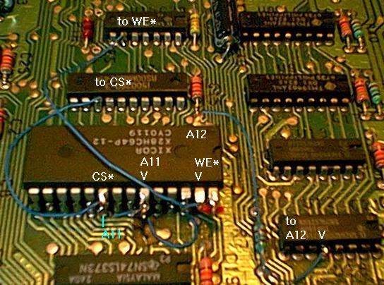
Here is a couple of pictures of a board using no switches: A12 goes to
the 74LS259 pin #12, and WE* goes directly to the 74LS02, pin #9. I got
you a view from the side, and a view from
the
top. Retrospectively, I realized that the
blue
wire I was using is a bit hard to see. I hope you can make out the
connections.
I marked the end points arrows. Note the the connections still need to
be insulated with electrical tape.
Have a critical look at your work. Are all connection clean? No solder bridge that will short-cut to neighbouring pins? Make sure connections to the stretched-out pins are trimmed and cleanly insulated with tape: They should not make contact with the metal casing, nor with the underlying PCB. Ditto for the switches if you installed any.
Now it's time to test your work. There is a small complication here: the TMS9902 chips on the board have the nasty habit to send interrupts until you tell them to shut up. The power-up routine that does so, as well as the routine that handles the interrupts, are in the card DSRs. However, since there is no DSR in the EEPROM yet, the interrupts will not be taken care of, and this will lock-up the TI-99/4A!
The remedy to this situation is very simple: take a tiny piece of electrical tape and cover connection #17 in the card edge connector (the one that goes into the PE-box slot). Connection #17 is the interrupt signal, it is the 9th connection from the rear, on the side of the card where the components are not.
Install the card into the PE-box. Leave the cover open and turn power-on. If you hear a small "bang", or if you smell smoke (or just a "hot smell"), turn the power off immediately are recheck your connections. Otherwise, wait for about 30 secs and turn power off. Touch the EEPROM with your finger: it should not be hot. Also check the other chips you have attached leads to.
Now power-up both the PE-box and the console: the TI-99/4A should start normally. If it's not the case, the most likely is that you did not mask the right connection with the tape, or that it got peeled away when you inserted the card. Otherwise, check your connections for a shortcut with a neighbouring pin.
If the TI-99/4A starts normally, all you have to do is to install the DSRs into the EEPROM. First, download the following zip file, and transfer its contents to your TI-99/4A as described in my donwload page. Then load the file RS/0 with an EA5 loader, like Editor/Assembler option 5, TI-writer, or Funnelweb.
Make sure to write-enable the EEPROM, then select the desired CRU: >1300 for an unmodified card, >1500 for a card doctored to answer a different CRU. The program will copy the file RS/1 into the EEPROM. It then offers you a chance to switch pages manually, or by toggling bit 7, and copies the file RS/2 into the second page.
The file RS/2 contains a patched DSR which automatically checks the console clock speed (from 2.5 MHz upto 6.0 MHz) and selects the proper baud rates, including 19200 and 38400 bauds. I also corrected a bug in the interrupt service routine so that you can now use the built-in timer. If you would like to have the patched version in both pages, repeat the above operations without actually switching pages. The source for the patch can be viewed here.
Once all this is done, you can remove the piece of tape that's
insulating
the interrupt connection. Make sure the TI-99/4A boots normally.
Finally, you may place the card back inside its metal case, if you
whish.
This is optional as the case was probably only intended by TI to
prevent
computer-illiterate people to put their fingers all over the PCB...
The console ROMs also suffer from a number of bugs and poor design decisions. For instance, there is a bug in the interrupt service routine that won't let us make use of the timer in the TMS9901 chip. Also, only three of the XOP vectors are installed. Finally, you may want to add some improvments of your own to the OS (such as multitasking...). There is not much space left in this memory area, unless you are willing to get rid of the cassette management routines: nowadays nobody uses cassette tapes anyway.
The hardware situation in the console is a little different from card ROMs. First, because the data bus is 16 bit-wide in the console. Which means that we have no alternative but to use two EEPROM chips, one for even bytes (D0-D7), one for odd bytes (D8-D15), just as is the case for the existing ROM chips. The good new is, since each chip is taking care of one byte we could use cheap Atmel EEPROMs. (NB I didn't because they were sold out, so I cannot guaranty that they would work. The B version was tested though, and it worked fine).
Second, because the ROM contains the boot sequence, we can't remove them. Sure we could place the boot code into an EEPROM, but how are we going to run the program that does it, if the computer won't boot? The solution is to have a switch that lets us toggle from ROM to EEPROM.
Finally, TI did not do a very good design job whith the ROMs: these chips answer both read and write operations! So instead of applying their selection line to the OE* pin of the EEPROM, we'll use it for the CS* pin, and we'll find an appropriate signal for OE*.
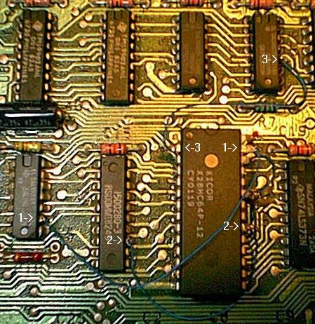
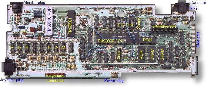
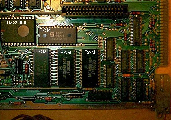
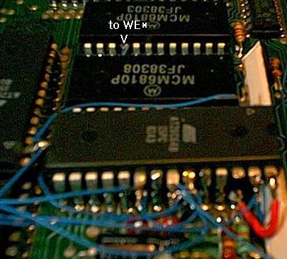
Refer to my console surgery page to open the console. Refer to this picture to indentify the components. The big mother chip in the middle is the TMS9900 microprocessor. Near to it are four wide chips (0.6 in), with 24 pins each , 12 on each side. Two of these chips are labeled 6810P: these are the scratch-pad RAM and you don't want to touch them. The other two, which are at 90` from each other, are the console ROMs. These are the ones on which we want to piggy-back the EEPROMs. Here is a blow-up of this region.
Here is a side view of the ROM chips, seen from its right side with
your eyes leveled to the board (which you can't actually do, but just
imagine
it):
                             ,------------- To switch, middle pole
    Bottom  .================|======, Top
             # # # # # # # # " # # #
To EEPROM pin 23-----'     |       '------ To EEPROM pin 28
                           '---------To switch, 2 opposite terminals
And here is a picture, note that the cut pins on the two ROMs have already been connected together (the wire goes under the first ROM).
The EEPROMs should now look like this:
             +---+--+---+
             | nc    Vcc|==-   To ROM pin #24
To switch -==| A12   WE*|==-   To 6810P RAM pin #16
or TMS9901  [| A7    nc |      (opt: via SPDT switch)
   pin #37  [| A6    A8 |]
or ground   [| A5    A9 |]
            [| A4    A11|==-   To ROM pin #18
            [| A3    OE*|==-   To 74LS04 pin #11
            [| A2    A10|]
            [| A1    CS*|==-   To DPDT switch, middle pole
            [| A0    D8 |]
            [| D1    D7 |]     Legend:
            [| D2    D6 |]     |==- Stretched-out
            [| D3    D5 |]     |    Cut
            [| Gnd   D4 |]     |]   Normal
             +----------+
Here is a picture. Note that the two EEPROMs are arranged in the configuration they should have once on the motherboard, (the side connector would be at the bottom).
Here is a picture of the first EEPROM, with most of the wires already attached (these will be discussed below). And here is a picture of the second EEPROM. Note that some insulating tape still needs to be added.
Pin #27 on either EEPROMs needs to be connected to WE*, a write-enabling pulsed signal. You will find this signal at pin #16 on either of the two 6810P RAM chips. First connect together pin #27 of both EEPROMs, then connect them to pin #19 of one of the RAM chips (visible on the previous picture).
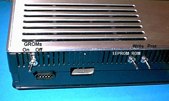
Optionally, you could install a SPDT write-protection switch on this line, with the following connections:
                               ,-------- both EEPROMs pin #27
one 6810P pin #16  ----------o_0 o---------- +5V
When the switch is to the left, the EEPROMs can be written to. When it's to the right, the chips are write-protected.
NB I strongly recommend that you install this switch. Initially I didn't do it and I found out the hard way that many programs do dummy writes in the ROM area (often at address >0000) and mess up the EEPROM.
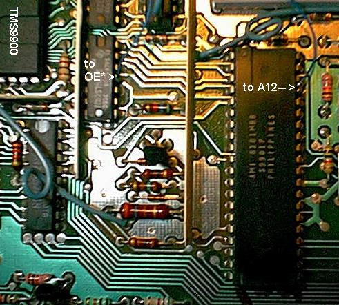
Pin #22 on either EEPROMs (OE*) needs to be connected to a signal
that's
active-low for read operations. You can find such a signal, DBIN*, at
many
places on the motherboard. A convenient location is on the 74LS04
that's
in the center of the board, near the TMS9901 (U602, see picture).
Solder the wire to its pin #11.
Pin #20 (CS*) should be connected to the other middle pole of the DPDT switch. The switch terminals should be connected to the same signal as the ROM portion of the switch, but in reverse orientation: two short pieces of wire will do the job.
In summary, the DPDT switch should be wired like this:
                    ,-------- both EEPROMs pin #20
+5V--------------o_0 o---------- ROM pin #20
ROM pin #20------o_o o---------- +5V
                   '--------- both ROMs pin #21
When the switch is on the left, the ROMs CS2* pin is controlled by the
same selection signal as the CS1* pin and the ROM is thus active. When
the switch is on the right, the EEPROMs are controlled by the selection
signal. The chips that are not controlled, are connected to +5V, which
disables them.
Finally, we need to deal with the extra address line A12 (pin #2). There are three solutions, outlined below:
1) If you are satisfied with 8K of EEPROM, you could just connect this pin to the ground: use a small piece of wire to connect pin #2 and pin #13 on each EEPROM. By doing so, however, you are loosing half the memory available in each EEPROM chip...
2) A better solution would be to install a SPDT switch that will let you select either half of the EEPROM chips. This way, you can have three versions of the console routines: one in ROM and two in EEPROM.
For this version, pin #2 on both chips should be connected together
and then to the middle pole of the SPDT switch.
Then connect one switch terminal to ground, the other to +5V. You will
find ground at the bottom left pin of any 74LSxxx chip, and +5V at the
upper right pin of these chips (or on your DPDT switch).
                    ,-------- EEPROMs pin #2
Ground ----------o_0 o---------- +5V
When the switch is on the left, it selects the lower 4K in each EEPROM. When it's on the right, it selects the upper 4K.
3) Yet another solution is to make use of one of the spare CRU bits in the console to switch pages by software. If you like the idea, connect pin #2 of both EEPROMs together, then to pin #37 of the TMS9901 interface controller (the wide, 40-pin chip that has no heat sink on top). It will answer to CRU bit 17, address >0022. This is the solution I chose: here is a picture (you've seen it before).
EEPROM pin   Goes to
28 (Vcc)     ROM pin #24 (+5V)
23 (A11)     ROM pin #18 (A11)
22 (OE*)     74LS04 pin #11 (DBIN*)
20 (CS*)     DPDT switch, middle pole
27 (WE*)     6810P RAM pin #16
             or middle pole of a SPDT switch
2  (A12)     ROM pin #12 (ground)
             or middle pole of another SPDT switch
             or TMS9901 pin #37
All others   Corresponding ROM pin
Connect the console. Make sure the DPDT switch is in "ROM" position and turn power on. If the console does not boot, or if you hear or smell anything suspicious turn power off immediately, re-open the console and check your connections.
When you put the switch in "EEPROM" position, the TI-99/4A won't boot since the EEPROMs are still empty. Any program running when the switch is toggled is likely to crash, since most rely on routines in the console ROMs (such as KSCAN, or the interrupt routine). Your next task will thus be to load a new version of the ROM routines into the EEPROM.
To do so, download the following zip file, and transfer its contents to your TI-99/4A as described in my download page. Then load the file ROMS/0 with an EA5 loader, like Editor/Assembler option 5, TI-writer, or Funnelweb.
Once loading is complete, toggle the switch to select the EEPROMs and make sure they are write-enabled, then press the spacebar (the program has it's own keyboard scanning routine). The program will automatically copy the file ROMS/1 into the EEPROMs. Be patient, as it can take quite a while...
The program then gives you a chance to flip the page switch, if you have one. Alternatively, it can toggles CRU bit 17 if you press <enter> instead of <space>. In any case, the file ROMS/2 will be copied in the second page, unless it's just a placeholder file, in which case ROMS/1 will be used again.
Revision 1. 9/14/01 RS232 only. Not tested yet. Not for release.